
HIGH-SPEED / SIGNAL INTEGRITY HIGHLEAP ELECTRONICS
14 Layer High Speed PCB Manufacturer in China for Low-Loss Designs
Highleap Electronics manufactures custom 14 layer high-speed PCBs in China for controlled-impedance, low-loss multilayer electronic designs. Our fabrication scope includes customer-specified dielectric systems, controlled signal and reference layers, precision via structures, selective backdrilling, appropriate surface finishes and PCB assembly when required. We coordinate the electrical stackup and the physical fabrication proposal so that the routed trace geometry corresponds to the dielectric and copper actually delivered.
Share your stackup, laminate requirements, impedance targets, backdrilling notes and production quantity.
14-Layer High-Speed PCB Materials, Stackup and Impedance
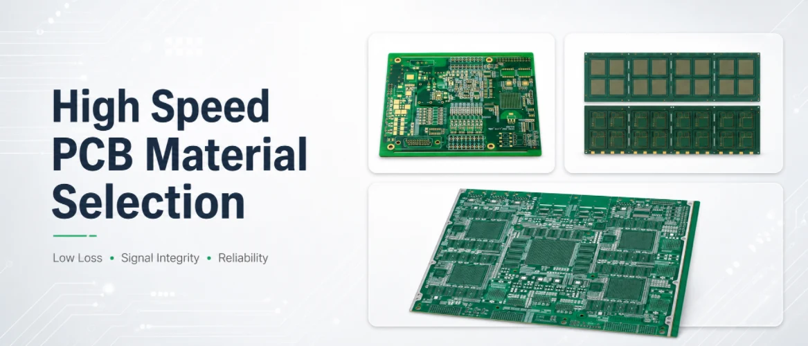
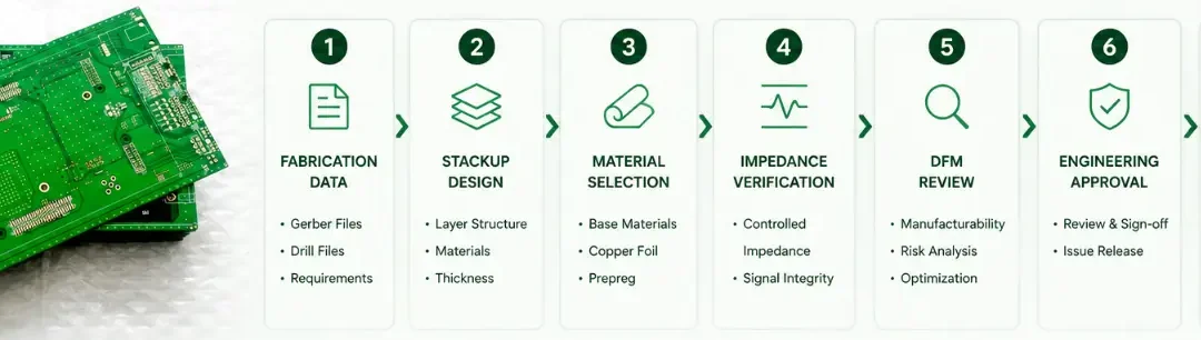
Highleap’s published multilayer rigid PCB capabilities include controlled impedance, high-layer-count construction and advanced drilling options. For a 14-layer high-speed build, the design review identifies the target material grades, controlled-impedance nets, finished copper dimensions, board thickness, via transitions and any special coupon tests. Production follows the customer-approved physical stack rather than a generic 14-layer stackup diagram.
The manufacturing scope may include traditional plated through-holes, buried connections, HDI, filled via-in-pad or targeted backdrilling; each is selected for its routing and electrical purpose. A project requiring a large controlled-loss network card and a compact processor module can share a fourteen-layer count while needing completely different laminate and hole constructions.
Can Highleap supply a high-speed board and a populated assembly?
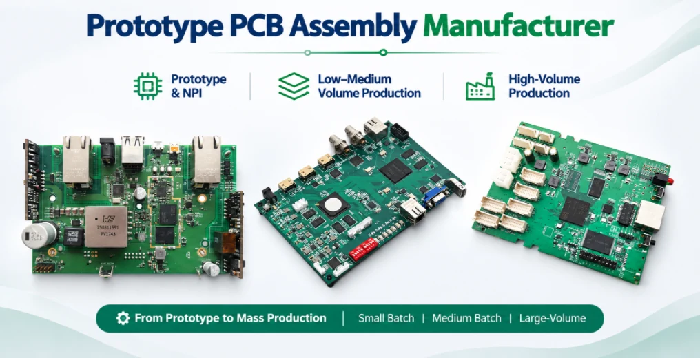
Highleap provides both PCB fabrication and PCB assembly services. For an integrated quotation, bare-board data are reviewed alongside the BOM, BGA footprint, connector placement and assembly drawings. Board-level test evidence such as impedance coupons must be distinguished from SMT X-ray inspection and system-level eye-diagram or packet-error testing, which require explicitly defined methods and equipment.
A 14-layer board built around high-speed channels is not selected by layer count alone. Where the same product can use a conventional rigid multilayer stack instead, the broader 14 layer PCB manufacturing options provide a useful basis for discussing process complexity before the signal-integrity requirements are finalized.
Low-Loss Laminates, Megtron Materials and Customer-Specified Brands
Material selection should be anchored to the electrical loss target and fabrication route. Candidate families may include Panasonic MEGTRON 6 and 7 families, approved Isola high-speed grades, Shengyi and ITEQ low-loss laminates, and selected Rogers materials for suitable hybrid structures. Highleap already describes Rogers and Panasonic materials within its PCB fabrication and material services; the exact grade, stock condition, copper foil and core/prepreg combination require order-specific confirmation.
| Material option | Engineering evaluation | Procurement action |
|---|---|---|
| High-Tg FR-4 | Thermal robustness; channel loss still needs independent verification. | Approve actual Dk/Df and assembly cycle. |
| MEGTRON / low-loss digital | Selected transmission-line loss targets at designated frequencies. | Confirm exact grade, core/prepreg, stocked or sourced. |
| Hybrid digital / RF stack | Only where approved dielectric systems can be bonded compatibly. | Review differential CTE, cure, registration and yield. |
| Copper foil profile | Conductor roughness influences insertion loss. | Specify foil and finished copper assumptions in modeling. |
High-Tg FR-4 is not automatically low-loss. Df depends on the material grade and test condition; Dk affects geometry and propagation. Low-profile or very-low-profile copper may reduce conductor loss, but foil choice also affects adhesion and processing. Where only certain layers carry sensitive channels, a qualified hybrid construction can be considered; different resin and core systems still need a compatible press and registration plan.
Does Megtron 6 automatically make a fourteen-layer PCB suitable for a 112G link?
No. A named low-loss laminate cannot guarantee an end-to-end link. The result depends on channel length, copper profile, glass style, transitions, connectors, package losses and equalization. The customer’s SI team must define its data-rate architecture and loss budget; manufacturing can then review the exact dielectric and conductor specifications and quote the relevant verification coupons.
Controlled Impedance, Dielectric Stackup and Trace Geometry
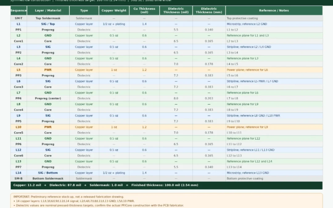
A fourteen-layer PCB may allocate signal layers next to continuous ground references while using separate copper planes for power delivery. Each critical net class needs a specified reference plane and permitted impedance range. The final trace widths are derived from pressed dielectric thickness, conductor cross-section, laminate properties and solder-mask loading, not from a universal “100-ohm pair” width. Highleap can review the release drawing with its controlled-impedance PCB process.
For each controlled structure, specify whether it is outer-layer microstrip, inner-layer stripline, broadside or edge-coupled differential routing, and identify the exact reference layers. If a trace changes layers, the return path must be maintained by the design with appropriate plane continuity and return transitions. A coupon design measures representative fabricated geometry, not the finished product’s entire signal channel.
What is included in a manufacturing impedance report?
For an ordered controlled-impedance build, agree the target value, allowable tolerance, representative coupon configuration, test method, sampling and report format. Time-domain reflectometry can evaluate the impedance of designated test structures. It does not, by itself, prove insertion loss, return loss, crosstalk or eye opening on every high-speed route. Channel-level S-parameter or system tests require an additional defined setup.
SerDes, PCIe, Ethernet Routing and Backdrilling
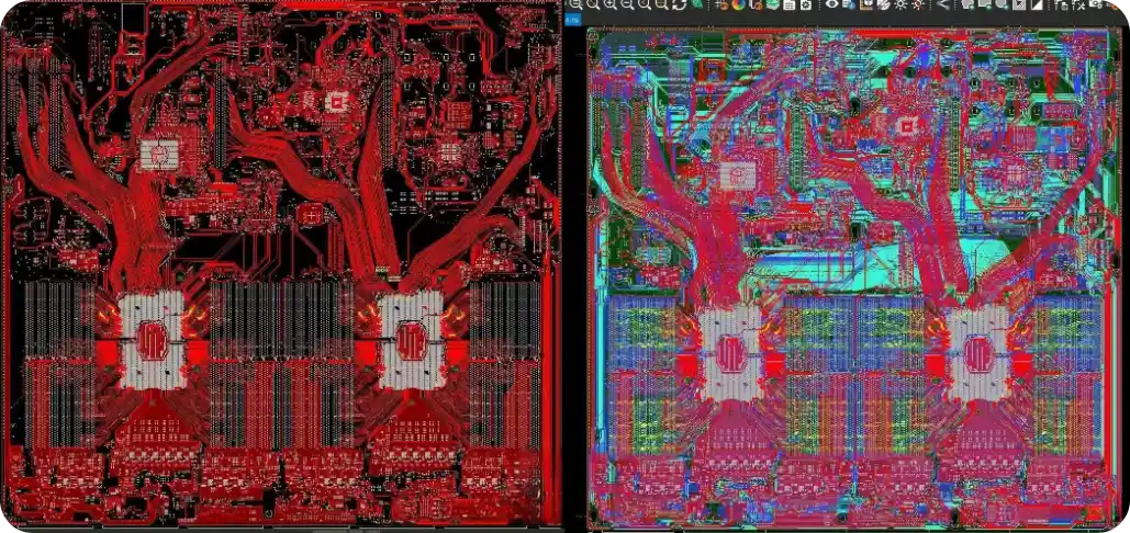
High-speed processor and network PCBs often contain SerDes lanes, Ethernet interfaces, PCIe buses, memory channels and clock distribution. Fabrication can preserve a routed design’s geometries, but the PCB supplier should not claim that one material automatically certifies PCIe Gen5/Gen6, DDR5 or a given Ethernet system. Such performance depends on the complete routed channel and system qualification.
Differential pair matching, skew control, return path and reference continuity must be frozen as part of the design; manufacturing changes to copper thickness, substrate dielectric or via geometry can modify those parameters. The handoff should distinguish fab-controlled dimensions from design-level signal integrity specifications such as length matching or crosstalk budgets.
How do glass weave and copper roughness affect a high-speed stackup?
Uneven glass/resin distribution can contribute to pair-to-pair dielectric variation, while rougher conductor profiles increase effective copper loss. Material glass style, fiber distribution and foil profile should be considered if the channel budget is sensitive. These effects cannot be resolved by applying the same “low Df” claim to every available laminate; the approved stackup and field model must use the intended material and copper construction.
Backdrilled Vias, BGA Escape and Connector Transitions
On a thicker multilayer PCB, a plated through-via can leave an unused stub beyond its connected signal layers. Backdrilling may reduce that discontinuity when the loss and return-loss budget justifies it. The backdrill drawing must identify drill side, target residual stub, hole diameters and clearances to active pads. Highleap’s backdrilling service is the relevant manufacturing process, not a universal operation on every 14-layer high-speed board.
When compact BGA escapes require microvias or via-in-pad, the dedicated HDI PCB manufacturing route is assessed against the package and assembly constraints, with additional construction information in our HDI PCB fabrication service. Buried/stacked microvias are distinct from mechanically drilled through holes; their risk, press cycles and inspection should be priced separately. For high-speed press-fit connectors, finished hole geometry and plating matter to both the connector manufacturer and the electrical channel.
Should every PCIe or SerDes transition be backdrilled?
No. Backdrilling is appropriate when an unused via barrel materially affects the channel and the mechanical depth clearance permits controlled removal. Short stubs or alternative via structures may already satisfy the electrical objective. The design authority should identify the transitions and acceptance limits, and the fabricator should confirm the drill and coupon/measurement scope.
High-Speed PCB Applications and PCBA Integration
Highleap can assess fourteen-layer PCB designs for Ethernet network-switch line cards, communication interfaces, server control and I/O cards, FPGA carrier boards, optical-transceiver interface modules and industrial compute platforms. These products share a need for controlled interconnects but differ in routing density and channel length. A short FPGA daughterboard may be dominated by escape routing; a longer network card can be dominated by dielectric loss and connector discontinuity.
Backplane-scale boards additionally require large-format handling, high-pin-count connectors and strict dimensional control. For a modular chassis with many daughter cards, our backplane PCB manufacturing service examines connector holes, board size and insertion fixtures beyond the signal-stack review; the broader backplane PCB fabrication capabilities cover other layer counts. The assembly program should confirm whether press-fit, soldered or mezzanine connections are required before the finished PCB construction is released.
High-Speed PCB Fabrication and Assembly Handoff
A populated high-speed board must preserve the intended electrical interfaces through soldering and connector installation. The PCBA quotation should identify BGA/QFN placement, component sourcing, X-ray of specified hidden joints, any cleaning/coating constraints and firmware or board-level test fixture needs. A connector manufacturer’s plated-hole acceptance can be as important as the bare-board impedance result where a press-fit or high-speed receptacle is used.
Our BGA PCB assembly service supports discussion of hidden-joint inspection, while functional testing covers separately agreed device-level checks. Neither is automatic proof of the specified high-speed interface compliance without customer-defined test limits.
Impedance Testing, Quality Control and Revision Management
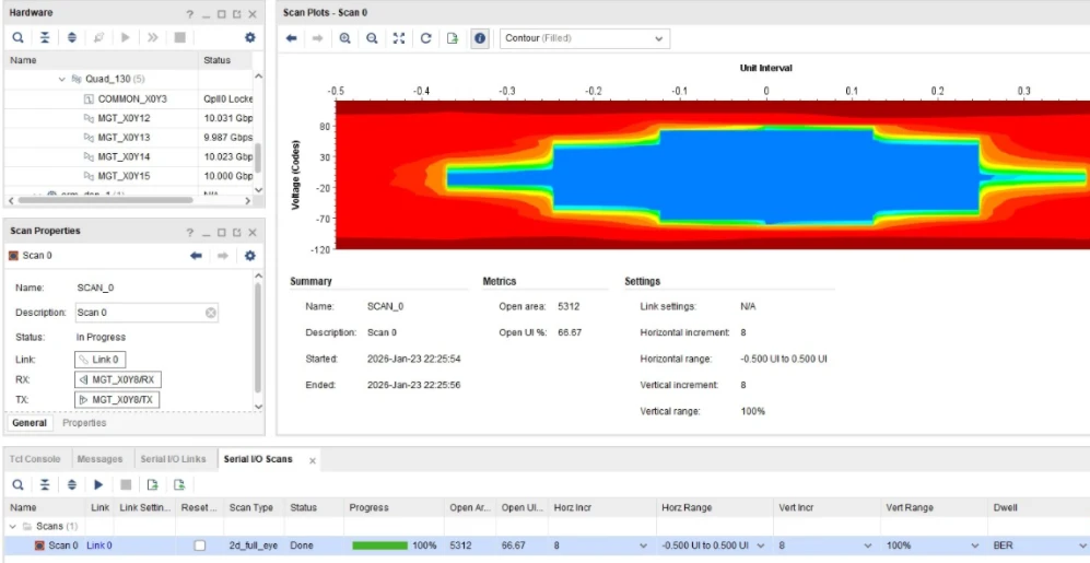
The fabrication acceptance plan may include inner-layer optical inspection, physical layer registration, mechanical-hole metallization checks, bare-board electrical continuity/isolation tests, controlled-impedance coupon readings and requested cross-sections. Any additional high-frequency insertion-loss coupons, high-speed channels or finished product tests must be included explicitly with the required test method and reporting format.
A repeat-production order should maintain the approved material grade, glass/resin style where controlled, copper foil profile, finished conductor dimensions, stackup revision and impedance coupon criteria. Changing any of these may require a revised field model or customer authorization. The applicable rigid-board workmanship standard and class belong in the fabrication order; a passing coupon does not replace end-system EMC or signal qualification.
Revision Control and Factory Qualification for High-Speed Production
A high-speed fabrication approval needs the physical stackup and not merely the electrical schematic revision. Record the permitted laminate manufacturer/grade, copper foil type, glass style if specified, finished conductor target, exact board thickness and coupons used for impedance acceptance. If the supplier proposes a substitute material, a new field solution or signal-integrity review may be needed before production is released.
For repeat orders, request the shipped lot number and the agreed fabrication report format. If critical channels have a loss requirement, document whether an insertion-loss test vehicle is included and how its results relate to the actual finished board. Manufacturing verification should not be conflated with a device-level pass/fail result from the customer’s network or compute tester.
Should the PCB manufacturer change trace width to recover the target impedance?
Only through an approved engineering change. Fabrication may propose width compensation based on the selected copper and pressed dielectric, but CAD geometry, spacing rules and pair coupling can constrain the adjustment. The OEM’s electrical design owner must approve any change that affects critical nets. For early engineering risk review, our PCB DFM service can identify conflicting design and production limits before artwork release.
What should be included in a high-speed PCB manufacturing acceptance package?
An appropriate acceptance plan identifies the material grade, stackup revision, copper construction, impedance table and test coupon design. It can also define differential-pair geometry, final trace/space criteria, backdrill remaining-stub target and the relevant test method. Depending on the contract, the supplied record may include netlist electrical testing, TDR impedance readings, selected dimensional results and microsection photographs of specified interconnect features. None of these is a direct measurement of the full assembled channel’s bit-error rate.
For demanding channels, system engineers may request material characterization at the design frequency or separate loss-coupon evidence. Those measurements should only be advertised as supplied after the test method, sampling, reporting format and equipment responsibility have been agreed. A 112G-capable electronic product is not proved simply by purchasing a board fabricated from a well-known low-loss laminate.
Lead Time and Cost Factors
A standard stocked high-Tg laminate construction can have a different delivery profile than a named low-loss material, a hybrid mixed-dielectric stack or a board needing backdrilling and extra channel measurements. Order-specific lead time must reflect the approved material supply, lamination and inspection plan. There is no defensible universal price for a “14-layer 100G PCB” without dimensions, material, quantity, interconnect structure and test scope.
For a better comparison between offers, use the same laminate grade, finished thickness, defined copper weights, connector-hole specifications and acceptance report requirements. The wider PCB fabrication pricing analysis addresses the cost structure; the actual price follows the released files and production quantity.
Request a 14-Layer High-Speed PCB Quote
Send the released Gerber/ODB++ files, layer order, physical stack or target thickness, exact material grade or approved alternatives, copper profile, impedance table and tolerance, channel/loss requirements, drill/backdrill maps, surface finish, quantities and required test reports. For populated boards, attach the complete BOM, placement data, mechanical interface drawing and program-level test plan.
Highleap can return a project-specific manufacturing review with the material and process assumptions clearly identified, including any changes that require the OEM’s technical approval.

Recommended Posts
14 Layer PCB Assembly and One-Stop PCB Fabrication
PCB FABRICATION + PCBAHighleap Electronics provides 14...
14 Layer PCB Stackup for High-Speed and Multilayer Manufacturing
ENGINEERING & STACKUP REVIEWA 14 layer PCB stackup is...
14 Layer PCB Cost: Fabrication, Prototype and Volume Pricing
PCB COST & QUOTATION14 layer PCB cost at Highleap...

AlN Ceramic PCB Manufacturer for High-Thermal-Performance Electronics
HIGHLEAP ELECTRONICS · Aluminum Nitride Ceramic PCB...
How to get a quote for PCBs
Let‘s run DFM/DFA analysis for you and get back to you with a report. You can upload your files securely through our website. We require the following information in order to give you a quote:
-
- Gerber, ODB++, or .pcb, spec.
- BOM list if you require assembly
- Quantity
- Turn time
In addition to PCB manufacturing, we offer a comprehensive range of electronic services, including PCB design, PCBA, and turnkey solutions. Whether you need help with prototyping, design verification, component sourcing, or mass production, we provide end-to-end support to ensure your project’s success.
For PCBA services, please provide your BOM (Bill of Materials) and any specific assembly instructions. We also offer DFM/DFA analysis to optimize your designs for manufacturability and assembly, ensuring a smooth production process.