
PCB Fabrication Cost Complete Pricing Guide

PCB fabrication cost varies dramatically based on design complexity, material choices, and production volume. Understanding these cost drivers enables engineers to make informed design decisions and procurement teams to budget accurately for their projects.
Table of Contents
At Highleap Electronics, we believe transparent pricing helps customers make better decisions. This guide breaks down the factors that influence PCB fabrication cost and provides practical strategies for optimizing your budget without compromising quality.
1. Understanding PCB Fabrication Cost Structure
PCB fabrication cost comprises multiple components that vary based on your specific requirements. Unlike commodity products with fixed pricing, circuit board manufacturing involves numerous variables that affect final cost.
The basic cost equation includes raw materials (laminate, copper, surface finish), manufacturing processes (drilling, plating, etching, imaging), testing and inspection, and overhead (equipment, labor, facilities). Each project presents a unique combination of these factors, which is why PCB quotes require detailed specifications rather than simple per-unit pricing.
Understanding this structure helps explain why seemingly small design changes can significantly impact cost. A board that looks simple might require expensive materials or complex processing, while a visually complex design might use standard processes that cost less than expected.
For a detailed breakdown of all cost components including assembly, see our comprehensive PCBA cost breakdown guide.
2. Material Costs: The Foundation of Pricing
Material selection often represents 30-50% of total PCB fabrication cost. Choosing appropriate materials for your application—neither over-specifying nor under-specifying—is crucial for cost optimization.
2.1 Base Laminate Options
Standard FR-4 remains the most cost-effective choice for most applications. This glass-reinforced epoxy laminate offers good electrical properties, mechanical strength, and thermal resistance at commodity pricing.
High-performance alternatives include high-Tg FR-4 (15-25% premium over standard) for elevated temperature applications, polyimide (3-5× FR-4 cost) for extreme temperatures or flex circuits, Rogers and other RF laminates (5-10× FR-4 cost) for high-frequency applications, and metal core (2-3× FR-4 cost) for thermal management.
2.2 Copper Weight Impact
Standard 1oz copper (35μm) is included in base pricing. Heavier copper increases cost through material cost (copper is priced by weight), processing difficulty (etching thick copper requires more time), and yield impact (thicker copper has tighter process windows).
Typical cost premiums run approximately 10-15% for 2oz copper, 25-35% for 3oz copper, and 50%+ for 4oz and heavier copper.
2.3 Surface Finish Selection
Surface finish affects both cost and performance:
- HASL (Hot Air Solder Leveling): Lowest cost, good solderability, not suitable for fine-pitch
- Lead-free HASL: Slightly higher cost than leaded, RoHS compliant
- ENIG (Electroless Nickel Immersion Gold): 20-30% premium, excellent for fine-pitch and wire bonding
- OSP (Organic Solderability Preservative): Low cost, limited shelf life
- Immersion Silver: Moderate cost, good for RF applications
- Hard Gold: Highest cost, required for edge connectors and high-wear contacts
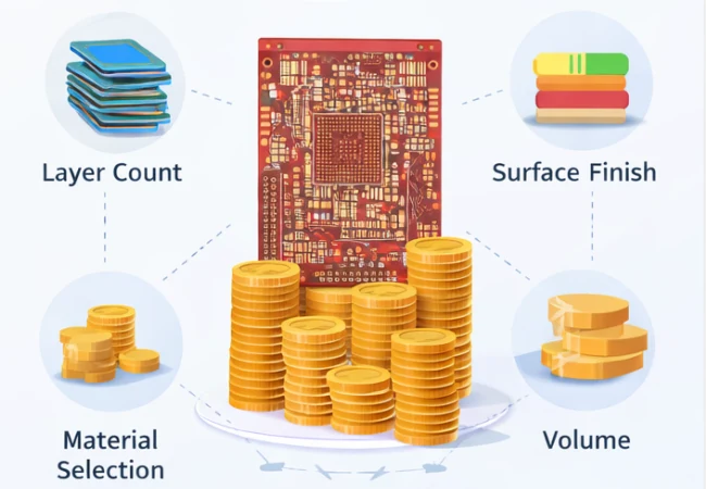
3. Design Complexity and Its Impact on Cost
Design choices made during schematic and layout phases significantly influence fabrication cost. Understanding these relationships helps optimize designs for cost-effective manufacturing.
3.1 Layer Count Economics
Each additional layer pair adds approximately 30-40% to base cost. This reflects additional material (core and prepreg layers), additional processing steps (imaging, plating, etching per layer), registration complexity (more layers = tighter alignment requirements), and yield impact (more opportunities for defects).
A 4-layer board typically costs 40-50% more than 2-layer. An 8-layer board costs roughly 2× a 4-layer board. Beyond 8 layers, consult our PCB manufacturing price per square inch guide for detailed multilayer pricing.
3.2 Minimum Feature Sizes
Tighter tolerances require more precise (and expensive) equipment and reduce manufacturing yield.
Standard capabilities (no cost premium) include 6/6 mil trace/space, 0.3mm minimum drill, and ±10% impedance tolerance. Advanced capabilities (15-30% premium) include 4/4 mil trace/space, 0.2mm minimum drill, and ±5% impedance tolerance. Leading-edge capabilities (50%+ premium) include 3/3 mil trace/space, 0.15mm laser drill, and ±3% impedance tolerance.
3.3 Via Types and Costs
Through-hole vias are included in standard pricing, but advanced via structures add cost. Blind vias add 20-40% as they require sequential lamination. Buried vias add 30-50% due to additional lamination cycles. Microvias add 40-60% as they require laser drilling. Via-in-pad with fill adds 25-40% for the filling and planarization process.
4. Volume Pricing: How Quantity Affects Cost
Production volume dramatically affects per-unit PCB fabrication cost due to setup amortization, material efficiency, and process optimization.
4.1 The Setup Cost Factor
Every PCB order involves fixed setup costs regardless of quantity: engineering review and CAM processing, tooling preparation (drill programs, imaging files), first article inspection, and test fixture setup.
These fixed costs—typically $100-500 depending on complexity—are amortized across the order quantity. For a 10-piece prototype order, setup might add $30-50 per board. For a 1,000-piece production order, setup adds less than $0.50 per board.
4.2 Typical Volume Price Breaks
Based on a standard 4-layer FR-4 board (100×100mm):
- Prototype (5-10 pcs): $2-30 per board
- Small batch (50-100 pcs): $5-15 per board
- Medium volume (500-1,000 pcs): $1-4 per board
- Production (5,000+ pcs): $0.5-2 per board
For projects with specific quantity requirements, review our PCB MOQ policies and low MOQ PCB assembly options.
4.3 Panel Utilization
Manufacturing panels are standard sizes (typically 18″×24″ or 21″×24″). Boards that efficiently fill panels cost less per unit than those with poor utilization. A 95×95mm board wastes significant panel space compared to 100×100mm—sometimes a slight size increase actually reduces cost.
5. Hidden Costs and How to Avoid Them
Beyond base fabrication cost, several factors can unexpectedly increase project expenses.
5.1 Design Rule Violations
Designs that violate manufacturer capabilities require either design revision (delaying schedule) or special processing (increasing cost). Common issues include insufficient annular rings, inadequate trace-to-edge clearance, and via-to-via spacing below minimum. Requesting a DFM (Design for Manufacturability) review before finalizing designs prevents these surprises.
5.2 Specification Creep
Over-specifying requirements inflates costs unnecessarily. Examples include requiring IPC Class 3 when Class 2 suffices, specifying controlled impedance on non-critical traces, and requesting 100% electrical testing when sampling is adequate. Match specifications to actual application requirements.
5.3 Rush Charges
Standard PCB lead time is typically 5-7 days for prototypes, 10-15 days for production. Expedited PCB manufacturing incurs significant premiums: 24-hour rush adds 100-200% to base cost, 48-hour rush adds 50-100%, and 72-hour rush adds 25-50%. Planning ahead avoids these premiums.
6. Strategies for Optimizing PCB Fabrication Cost
Practical approaches to reduce PCB fabrication cost without compromising functionality:
6.1 Design Optimization
- Right-size your board: Smaller boards cost less; optimize component placement to minimize area
- Minimize layer count: Each layer pair adds 30-40%; creative routing can often reduce layers
- Use standard features: Standard drill sizes, trace widths, and spacing reduce cost
- Design for panelization: Consider panel utilization during layout
6.2 Material Selection
- Use FR-4 when possible: Only specify high-performance materials when technically required
- Optimize copper weight: Use heavier copper only where current capacity demands it
- Choose appropriate finish: Match surface finish to assembly and reliability requirements
6.3 Volume Planning
- Consolidate orders: Combine multiple designs on one panel when possible
- Plan for volume: Consider future production needs when designing prototypes
- Balance MOQ and unit cost: Sometimes ordering slightly more reduces per-unit cost significantly
6.4 Supplier Partnership
Working with an experienced manufacturer like Highleap Electronics provides DFM review identifying cost reduction opportunities, material recommendations based on application requirements, volume pricing optimization, and combined PCB assembly cost savings through integrated fabrication and assembly.
For projects requiring both PCB fabrication and assembly, our PCB fabrication services integrate seamlessly with assembly operations, reducing handling, lead time, and total project cost.
Contact our engineering team to discuss your specific requirements and receive a detailed quote optimized for your application and budget.

Recommended Posts
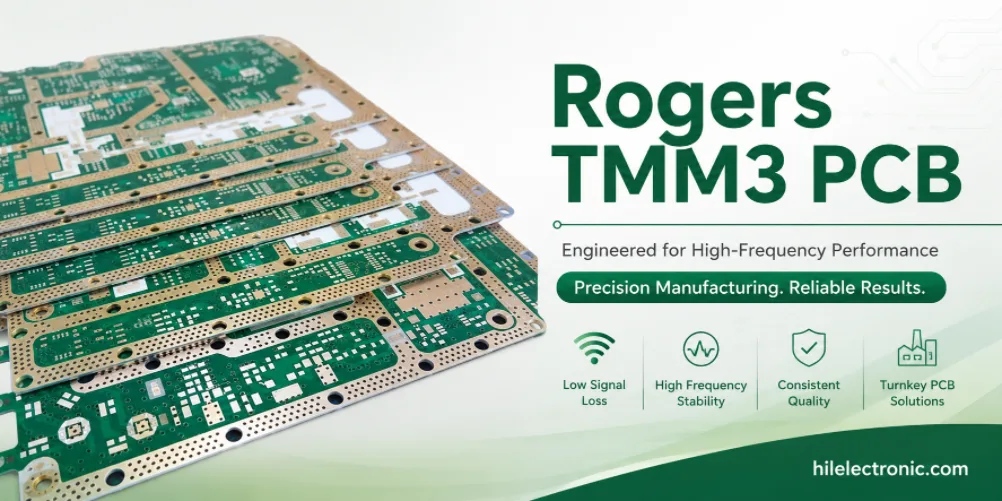
Rogers TMM3 PCB Manufacturer for Mechanical RF Modules
TMM3 is selected when an RF circuit must behave as part of...
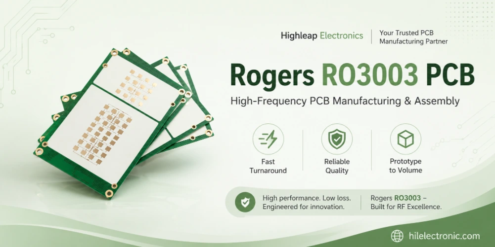
Rogers RO3003 PCB Manufacturer for Automotive Radar and mmWave Modules
A 77 GHz radar board is purchased as a working sensor...
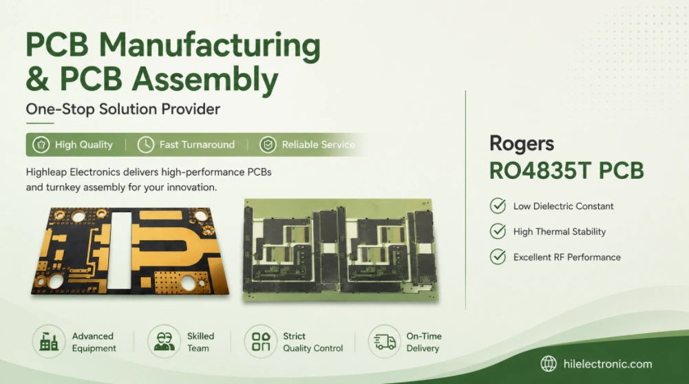
Rogers RO4835T PCB Manufacturer for Thin-Core RF Multilayer Boards
RO4835T is useful when the RF layer must move inside the...
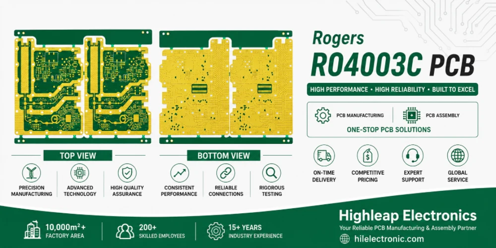
Rogers RO4003C PCB Manufacturer for RF and Hybrid Multilayer Boards
RO4003C is often the point where an RF project stops...
How to get a quote for PCBs
Let us run DFM/DFA analysis for you and get back to you with a report.
You can upload your files securely through our website.
We require the following information in order to give you a quote:
-
- Gerber, ODB++, or .pcb, spec.
- BOM list if you require assembly
- Quantity
- Turn time
In addition to PCB manufacturing, we offer a comprehensive range of electronic services, including PCB design, PCBA (Printed Circuit Board Assembly), and turnkey solutions. Whether you need help with prototyping, design verification, component sourcing, or mass production, we provide end-to-end support to ensure your project’s success. For PCBA services, please provide your BOM (Bill of Materials) and any specific assembly instructions. We also offer DFM/DFA analysis to optimize your designs for manufacturability and assembly, ensuring a smooth production process.