
Back to blog
Factors That Affect Rigid-Flex PCBs Cost

What Are Rigid-Flex PCBs?
Rigid-flex PCBs are a sophisticated technology that marries the durability and support of rigid PCBs with the flexibility and adaptability of flexible circuits. This hybrid approach allows designers to create electronics that can fit into unique shapes and spaces, offering significant advantages over traditional PCBs in terms of design flexibility, performance, and space utilization.
Special Structure of Rigid-Flex PCBs
- Layer Composition: Rigid-flex PCBs consist of multiple layers, including rigid layers that provide structural stability and flexible layers that allow bending and folding. This composition enables the PCB to be partially flexible, accommodating complex installation requirements or movement during use.
- Flexible Interconnects: The flexible sections serve as high-reliability interconnects between the rigid areas of the PCB. This eliminates the need for connectors and cables, reducing the overall size and weight of the product and enhancing reliability by reducing the number of potential failure points.
- Integrated Construction: Unlike simply attaching a flexible PCB to a rigid one, rigid-flex PCBs are built as a single unit. The transition between rigid and flexible layers is seamless, which is crucial for maintaining signal integrity and mechanical performance.
- Customizable Layer Stack-up: The layer stack-up in a rigid-flex PCB can be highly customized to meet specific electrical and mechanical requirements. Designers can adjust the number of layers, their thickness, and the materials used based on the application’s needs.
- Protective Finishes: Rigid-flex PCBs often feature protective finishes and coverlays to shield the flexible sections from environmental factors, such as moisture and abrasion, which could otherwise degrade performance over time.

Material Selection’s Impact on Rigid-Flex PCBs Costs
Base Material:
The most common base material for the flexible part of a rigid-flex PCB is polyimide due to its excellent thermal stability, flexibility, and electrical properties. An alternative, cheaper material might be polyester, which also offers good flexibility but with lower thermal resistance and durability.
Copper Cladding:
Copper is used for the conductive layers, and its thickness can vary. Standard thicknesses include 1 oz, 2 oz, and higher for different applications. The cost increases with thickness due to the use of more copper.
Layer Count affect Rigid-Flex PCBs Costs
Materials:
Each additional layer requires more substrate material, conductive (copper) layers, and prepreg (the bonding material between layers), directly increasing material costs.
Manufacturing Processes:
More layers necessitate additional steps in the manufacturing process, including lamination, drilling, plating, and etching for each added layer. These steps increase the time and complexity of production, leading to higher labor and overhead costs.
Yield and Waste:
With increased layer count, the probability of defects rises, potentially lowering the yield (the percentage of fully functional boards produced). A lower yield means more material and time must be devoted to producing a given number of acceptable boards, indirectly increasing costs.
Size and shape
Material Usage: The most direct impact of the PCB size is on the amount of material required. Larger PCBs use more substrate material, conductive layers (such as copper), and protective coatings, directly increasing the material cost.
Processing: Larger PCBs can also require special handling and processing steps, further adding to the cost. For example, larger boards may need additional support during the manufacturing process to prevent warping or damage, and they may also incur higher costs for inspection and testing.
Complexity: Irregular shapes or designs with intricate cutouts and contours can increase manufacturing complexity. Specialized cutting and machining processes are often required to achieve non-standard shapes, increasing production time and costs.
Tooling and Setup: Custom shapes might require unique tooling or fixtures, leading to higher setup costs. These costs are especially significant for low-volume runs where the setup costs are a larger proportion of the overall manufacturing expense.
Panelization Efficiency: The efficiency of panelization is also affected by the PCB’s shape. Standard rectangular boards can be easily arranged to maximize panel usage, reducing waste. In contrast, irregular shapes may leave unused spaces on the panel, which cannot be used for other PCBs, thus increasing the per-unit cost.
Wastage: Similar to size, the shape of a PCB can affect the amount of waste material produced during manufacturing. Designs that result in higher wastage will inherently be more costly due to inefficient material use.
If this requirement affects sourcing or production release, compare it with PCB material selection and PCB component selection before sending the final files for review.
Special Features Impact on Rigid-Flex PCBs Costs
1. Impedance Control:
Impact: Ensuring impedance control requires precise calculations and adjustments to the PCB’s geometry (trace width, spacing, and dielectric thickness) and material properties. This precision level often necessitates additional design time, specialized materials, and testing to verify compliance with the required impedance values.
Cost Implications: The need for high precision and additional testing can increase the cost by 10-20% compared to standard designs, depending on the complexity and the specific impedance requirements.
2. Blind and Buried Vias:
Impact: These vias connect internal layers without going through the entire board (blind vias) or connect two or more internal layers (buried vias), enabling more complex designs without increasing the PCB size. Manufacturing them involves additional drilling and plating steps, which must be precisely aligned across multiple layers.
Cost Implications: Incorporating blind and buried vias can increase costs by 15-30%, influenced by the number of vias, their sizes, and the complexity of the layer stack-up.
3. Through-Hole Plating:
Impact: Through-hole plating is essential for creating reliable connections between PCB layers but requires precise drilling followed by electroplating. This process is resource-intensive, especially for boards with high layer counts or small drill sizes.
Cost Implications: The addition of through-hole plating can raise production costs by 10-25%, depending on the complexity of the design and the volume of holes required.
4. Rigid-Flex Transitions:
Impact: The areas where rigid PCBs transition to flexible circuits are critical points that require careful design and manufacturing to ensure reliability and durability. These transitions often require specialized materials and additional processing to prevent stress and wear.
Cost Implications: The complexity of managing rigid-flex transitions can add 20-40% to the cost, primarily due to the specialized design considerations and the need for precise manufacturing and testing.
5. High-Density Interconnects (HDI):
Impact: HDI technology allows for a higher density of components on a PCB by using smaller vias and pad sizes. While HDI can significantly increase the functionality of a PCB in a smaller space, it requires advanced manufacturing techniques, including laser drilling and fine-line etching.
Cost Implications: Incorporating HDI features can lead to a 25-50% increase in costs, driven by the need for specialized equipment, materials, and the increased complexity in the manufacturing process.
Testing and Quality Requirements
Prototype Testing: Early-stage testing to identify design or functionality issues. While necessary, it can be costly due to the low volume of units produced and the high level of manual inspection and testing required.
Production Testing: Applied to each unit or a sample batch during the production run. Economies of scale can reduce the impact on the per-unit cost, but the comprehensive nature of required tests (electrical, AOI, etc.) adds to the overall expense.
Quality: The level of testing required is often dictated by the application of the PCB. High-reliability sectors (aerospace, medical, automotive) necessitate more rigorous testing, which increases costs but is justified by the need for near-perfect reliability.
Tips for Reducing Rigid-Flex PCBs Cost
- Use the least number of layers possible
- Design with standard materials and processes in mind
- Reduce board size as much as possible
- Use lower cost stiffener materials where feasible
- Build panels efficiently to maximize material utilization
- Adjust layer stackup to standard thicknesses when possible
- Consider longer lead times for best pricing
- Order larger quantities to benefit from volume discounts
- Design for ease of manufacture and assembly where practical
- Engage with your PCB partner early in design process
- Request design reviews to identify cost reduction opportunities

Related Articles
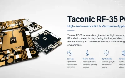
Taconic RF-35 PCB Manufacturing Service — Prototype Through Volume Production
Taconic RF-35 PCB manufacturing — ORCER family organic ceramic board fabrication from prototype to volume production with engineering DFM review.
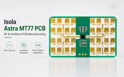
Isola Astra MT77 PCB Manufacturing
Isola Astra MT77 PCB manufacturing for RF, microwave and mmWave boards. Highleap supports DFM, impedance control, HDI, VIPPO, PCBA and after-sales service.
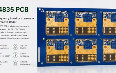
Custom Rogers RO4835 PCB Fabrication & Assembly Services
Highleap Electronics offers custom high-frequency fabrication, controlled impedance, hybrid stackups, and turnkey SMT assembly. Get a quote!