
Back to blog
The Ins and Outs of PCB Drilling: A Complete Guide

PCB drilling stands as a pivotal stage in PCB fabrication, pivotal for perforating holes facilitating component integration and interconnection among diverse circuit layers. This comprehensive guide aims to furnish PCB designers, engineers, and manufacturers with an exhaustive understanding of the intricacies surrounding the PCB drilling process.
Our discourse encompasses a wide array of PCB hole intricacies – from conventional types like Plated Through Holes (PTH) and buried vias to specialized variants such as backdrilled vias. Delve into the latest drilling methodologies, imperative process parameters, stringent quality control benchmarks, and adept strategies for enhancing hole fabrication.
Upon completion, you’ll attain an extensive comprehension of:
- The pivotal role and indispensable significance of PCB drilling in the realm of electronic manufacturing.
- State-of-the-art PCB drilling methodologies and sophisticated equipment driving contemporary practices.
- Methodical setup and meticulous execution of the drilling process to yield superior quality outcomes.
- Varied categories of PCB holes along with meticulous considerations dictating their design.
- Stringent benchmarks employed for evaluating the quality and precision of drilled holes.
- Insightful strategies for mitigating common drilling challenges and optimizing the overall process for enhanced efficiency.
Armed with this pragmatic compendium, PCB designers can adeptly craft manufacturable board layouts, engineers can meticulously oversee production processes, and fabricators can refine their drilling prowess to meet exacting industry standards. Let’s embark on an enlightening journey to unravel the quintessence of PCB drilling!

PCB Via Hole Types
PCBs feature a variety of via hole types, each serving distinct mechanical and electrical purposes. Despite all being physically “drilled,” their definitions, fabrication steps, and design considerations differ significantly. Here are the major categories:
Plated Through Holes (PTH)
PTHs traverse the entire PCB thickness, with conductive metal plating on their internal walls. This enables component leads to pass through and connect circuits on different layers. PTH dimensions, pad sizes, and plating thickness all impact manufacturability.
Non-Plated Through Holes (NPTH)
NPTHs are unplated vertical holes in a PCB, primarily used for installing mechanical fasteners like screws, spacers, and supportive pins. Adequate spacing from internal circuitry must be ensured.
Blind/Buried Vias
Blind vias terminate at an internal layer, while buried vias are encapsulated internally. Both types do not span the full PCB thickness, requiring advanced drilling and layer stacking. High-density designs often utilize many blind/buried vias.
Micro Vias
These are small vias with diameters below 150um, used to transit between adjacent layers. Fabrication involves specialized laser/mechanical drilling to hit tolerances. Micro vias save space and cost versus traditional vias in multilayer boards.
Fastener Holes
Fastener holes provide openings for screws, bolts, and other hardware to mount PCB assemblies. Proper spacing from traces and pads is necessary to avoid interference with electrical components.
Mounting Holes
These holes are reserved for attaching the completed PCB assembly to external mechanical structures.
Backdrilled Holes
Backdrilled holes are plated through holes with controlled depth drilling to remove the upper half of the plated barrel after initial full-depth drilling. This minimizes the risk of unwanted stubs causing impedance discontinuities in high-frequency signals, thereby enhancing circuit performance.
Via-in-Pad
Vias in Pad are plated through hole vias intentionally designed to overlap with component soldering pads. This allows vertical transitions through vias underneath mounted components, enhancing mechanical alignment integrity.
Filling Vias
Via filling involves inserting conductive or non-conductive epoxy material into vertical interconnecting holes after initial drilling and plating. Epoxy filling can be partial or complete, filling up the entire via barrel.
Half-Holes
Plated half-holes, or castellated holes, are rows of holes drilled alongside the boundaries of a rigid PCB. They are through plated and milled off half, mainly used for board-on-board connections.
Thermal Vias
These simple plated through holes are located under surface-mounted heat source components on a PCB. They establish a low thermal resistance path from the top copper to the bottom side of the PCB, aiding in heat transfer. Thermal vias often require an array of vias for effective heat dissipation.
PCB Drilling Methods
PCB drilling methods play a crucial role in determining the efficiency, precision, and cost-effectiveness of the drilling process. Here are the main methods used in the industry:
Automated Drilling
Automated drilling is ideal for high-volume production, utilizing rigs with programmable direct numerical control (DNC). These machines can perform multi-spindle simultaneous operations, ensuring fast cycle times and low cost per hole. However, they have limitations in terms of hole size upper limits and material flexibility.
Manual Mechanical Drilling
Manual mechanical drilling involves the use of milling machine beds with adjustable X-Y tables. While slower than automated drilling, this method is versatile and well-suited for quick-turn prototypes with customizable hole patterns. Precision is influenced by operator skill, with a higher risk of human errors compared to automated methods.
Laser Drilling
Laser drilling offers the capability to create extremely small hole diameters, down to less than 50 micrometers. This method minimizes mechanical stresses, reducing the risk of microcracking issues. Laser drilling provides excellent depth control but is slower than mechanical processes. Its main limitation is the requirement for line of sight access to the target hole location.
Each drilling method has its advantages and limitations, and the choice depends on factors such as production volume, hole size requirements, material properties, and budget considerations. Understanding these methods allows PCB manufacturers to select the most suitable drilling approach for their specific needs, balancing speed, precision, and cost-effectiveness.
PCB Board Material Selection
Selecting the right PCB board material is crucial for the drilling process, as it directly impacts the quality of the drilled holes. Several key factors come into play when choosing the material:
-
Brittle Substrates: Some substrates are more prone to microcracking under drilling stresses. Using pre-drill backups can help prevent crack propagation and maintain the structural integrity of the board.
-
High Tg Materials: Materials with a high glass transition temperature (Tg), such as polyimide, can withstand high temperatures. However, their poor thermal conductivity can lead to heat concentration, necessitating peck drilling to mitigate this issue.
-
Thick Copper Layers: Boards with thick copper layers and unfinished foil surfaces can cause faster wear on drill flutes. Using lubricants can help reduce friction and aid in chip clearance during drilling.
When it comes to drilling documentation, drill data files are essential for optimizing the drilling process. These files consider factors such as total hole count, hole density, hole size distribution, position accuracy requirements, and via-in-pad constraints to balance production needs and capabilities effectively.
Equipment and tooling selection are critical aspects of the drilling process. The choice between mechanical drills and laser/etching drills involves trade-offs in taper control, small diameters, and material compatibility. Additionally, drill bit properties, such as geometrical parameters and tool-life considerations, must be carefully evaluated. Support tooling, including backup plates, parameter guides, and vertical stops, also play a crucial role in ensuring the success of the drilling process.
Considerations For Selecting Drills In PCB Drilling
When selecting drills for PCB drilling, several considerations are crucial to ensure the fabrication process meets design intent:
- Drill Diameter: Match drill sizes to component lead widths and maintain adequate annular ring distances for soldering joints. Account for hole tolerance and drill accuracy variations, considering the board thickness to avoid drill walking.
- Aspect Ratio: High depth to diameter proportions can cause plating and reliability risks. Target a 10:1 ratio for typical through holes as a guideline to minimize these risks.
- Depth Control of Blind/Buried Vias: Optimize layer transitions with staggered depths, as lower ratios simplify plating throwing power needs and enhance reliability.
- Specialist Micro Drills for Dense Packaging: Laser drilling extends capabilities below 0.15mm, enabling tight process controls for modern HDI designs.
Collaboration with fabrication partners is key to drill selection. Understanding the plant’s capabilities, measured tolerance data, and depth limitations can help define appropriate drill sizes and ensure successful PCB fabrication.
Key Quality Metrics in PCB Drilling

Maintaining high-quality holes is essential for the reliable functioning of printed circuit boards (PCBs). Several key metrics are used to evaluate the quality of drilled holes:
- Hole Position Accuracy:
- Measures the difference between the designed and drilled hole center.
- Influenced by the precision of drill guides.
- Typical tolerance is ±0.05 mm.
- Hole Diameter:
- Checks the actual hole size against the specified size.
- Affected by tool wear and machine parameters.
- Standard tolerance is ±0.025 mm.
- Circularity:
- Indicates the roundness of the hole.
- Calculated as the ratio of the maximum and minimum hole diameters in perpendicular axes.
- A value close to 1 indicates high circularity.
- Barrel Hole Wall:
- Refers to the taper or hourglass shape of the plated hole.
- Caused by non-uniform plating thickness.
- Can impact the resistance of the hole.
- Hole Breakout:
- Occurs as separation around the hole exit on the outer layer.
- Caused by the drill penetrating the last laminate.
- Can affect the quality of pad connections.
- Drill Smear:
- Refers to resin debris redeposited on the hole wall after drilling.
- Impacts the adhesion and conductivity of copper plating.
By optimizing the drilling process and closely monitoring these metrics, PCB manufacturers can ensure the production of high-quality holes with the correct size, placement, and profile, leading to reliable PCBs.
Recent Advances in PCB Drilling Technology
In the ever-evolving landscape of PCB manufacturing, recent advancements in drilling technology have significantly enhanced precision, efficiency, and throughput. These developments represent a convergence of cutting-edge techniques and state-of-the-art equipment tailored to meet the exacting demands of modern PCB designs. Here is an overview of key advancements:
- Laser Drilling for Microvias: Laser drilling has emerged as a cornerstone technology for creating microvias with unprecedented precision, enabling diameters as small as 0.008 mm in HDI (High-Density Interconnect) boards. This technique facilitates intricate routing and miniaturization, vital for compact electronic devices.
- Plasma Drilling with High Aspect Ratios: Plasma drilling offers superior aspect ratios of up to 10:1, surpassing traditional drilling methods. This capability enables the creation of deeper holes with minimal diameter deviation, enhancing the versatility of PCB designs.
- Automated Optical Inspection Systems: Advanced optical inspection systems have been integrated into PCB drilling processes to provide real-time, in-line analysis of hole quality. These systems utilize sophisticated algorithms to detect defects, ensuring compliance with stringent quality standards and minimizing production errors.
- In-Process Cleaning Systems: Innovative in-process cleaning systems have been developed to mitigate debris accumulation during drilling operations. By removing contaminants in real time, these systems optimize drilling performance and prolong tool life, resulting in consistent hole quality.
- Predictive Tool Condition Monitoring: Leveraging power and acoustic sensors, predictive monitoring systems continuously assess drill bit condition during operation. By detecting early signs of wear or damage, these systems preemptively trigger maintenance actions, ensuring uninterrupted production and preserving hole integrity.
- Multi-Station Machines for High Throughput: Next-generation drilling machines feature multi-station configurations equipped with up to 152 spindles. This design maximizes throughput and efficiency, enabling simultaneous drilling operations on multiple PCB panels without compromising accuracy.
- Reduced Lubrication Spindles: Innovative spindle designs incorporating reduced lubrication requirements have emerged, offering environmental benefits while maintaining optimal performance. These spindles minimize lubricant consumption by up to 75%, reducing operational costs and ecological footprint.
- Automated Drill Wear Compensation: Advanced compensation mechanisms automatically adjust drilling parameters to compensate for tool wear, ensuring consistent hole dimensions throughout the production process. This proactive approach to maintenance enhances process stability and yields high-quality PCBs.
Collectively, these advancements represent a paradigm shift in PCB drilling technology, empowering manufacturers to achieve unparalleled precision, scalability, and reliability in their production processes. As the industry continues to push the boundaries of innovation, these technologies will play a pivotal role in shaping the future of electronic manufacturing.
For production planning, it also helps to compare this topic with PCB material selection and surface finish comparison before finalizing the fabrication or assembly package.
How Highleap CAM Engineers Handle Drilling Files

Highleap’s CAM engineers are committed to ensuring the quality and manufacturing efficiency of PCB drilling files. Here is a general overview of the steps and methods they use to handle PCB drilling files:
- File Inspection and Preparation: The CAM engineers begin by thoroughly inspecting the PCB design files, including Gerber and drilling files, to ensure completeness, accuracy, and compliance with design requirements. They carefully check the number of holes, hole sizes, tolerances, and hole attributes for consistency. They also verify that the drill symbols layer contains holes and that slot hole files are not mistakenly converted into drill files. Any discrepancies are promptly communicated with the designer. This attention to detail is a key advantage of choosing a PCB manufacturer with one-on-one engineering support.
- Engineering File Processing: Once the design files are verified, they are loaded into CAM software. The CAM software processes the drilling files, translating the design data into machine-readable instructions for the drilling equipment. After verifying the accuracy of the drilling files, the CAM engineers compensate for the drill holes based on surface treatment, board thickness, and Highleap Electronic’s process specifications. For complex PCB designs, such as those requiring dense vias, non-standard operations such as moving and shrinking holes may be necessary. This is why PCB designers need to understand the manufacturer’s process capabilities in advance, and why it is important to choose a manufacturer with experienced engineers.
- Drill Tool Selection: Based on the PCB design requirements and manufacturing processes, the CAM engineers select the appropriate drill tools. Factors such as drill bit sizes, materials, and coatings are considered to ensure precise and efficient drilling.
- Process Optimization: The CAM engineers optimize the drilling process to improve efficiency and quality. This includes optimizing drilling sequences to minimize tool changes and reduce cycle times. They also adjust drilling parameters such as spindle speed, feed rate, and peck depth to achieve the desired hole quality and production efficiency.
- Quality Control: Stringent quality control measures are implemented to ensure the accuracy and quality of the drilled holes. Automated optical inspection (AOI) systems are used to verify the dimensions and positions of the drilled holes, ensuring they meet the design specifications. Any deviations are identified and corrected promptly to maintain quality standards.
- Generation of Manufacturing Files: Once the drilling files have been processed and verified, the CAM engineers generate the final manufacturing files. These files contain precise instructions for the drilling equipment, ensuring that the PCBs are drilled accurately and efficiently during the manufacturing process. Special requirements are clearly noted in the ERP system for traceability and reference.
By following these meticulous steps, Highleap’s CAM engineers ensure that PCB drilling files are processed with the highest level of accuracy and quality, resulting in PCBs that meet design specifications and manufacturing standards.
conclusion
The world of PCB drilling is a dynamic and intricate domain, playing a crucial yet often unseen role in seamlessly integrating components across electronic devices. From meticulously processing design files and optimizing drilling parameters, to implementing stringent quality control measures, CAM engineers undertake a multifaceted process guided by precision, efficiency and reliability. Their expertise ensures design specifications and manufacturing standards are consistently fulfilled through each step.
As the electronics industry continues its rapid advancement, so too does the landscape of PCB drilling evolve. Recent innovations like laser microvia formation and automated optical inspection have revolutionized capabilities, pushing boundaries of what is possible. With continued commitment to excellence from CAM engineering teams, the future promises further breakthroughs that will shape manufacturing. Through collaboration, innovation and dedication to quality, the PCB sector is poised for ongoing transformation. By driving progress in drilling technologies, the industry will continue powering innovation across the world of electronics for years to come.
Overall, the work of CAM engineers remains an integral yet underappreciated foundation supporting functionality across devices ubiquitous to modern life. Their commitment to optimizing drilling processes amid rising complexity ensures smooth advancement today and tomorrow.

Related Articles
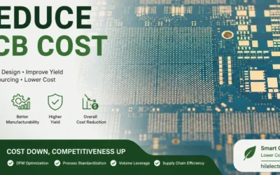
How to Reduce PCB Costs in 2026
Practical ways to reduce PCB costs in 2026 through material right-sizing, hybrid stackups, layer-count discipline, DFM yield improvement, copper control and panel utilization.
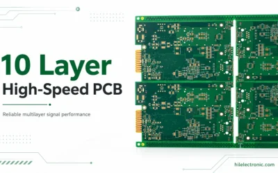
10 Layer High-Speed PCB Engineering for DDR5 and PCIe
Engineering guidance for 10 layer high-speed PCB projects using DDR5, PCIe, CXL and high-rate channels, including loss budgets, vias, stackup and verification.
10 Layer PCB Impedance Control and TDR Verification
A practical guide to 10 layer PCB impedance control, covering stackup inputs, field-solver geometry, manufacturing tolerance, coupons and TDR verification.