
Back to blog
How to Optimize and Reduce PCB Size: A Comprehensive Guide

In today’s world of compact and technologically advanced products, the size of printed circuit boards (PCBs) plays a crucial role in determining the success of electronic designs. The optimization of PCB size is not merely a matter of aesthetics but has far-reaching implications on manufacturing costs, product dimensions, and even the performance of the electronic devices. This comprehensive guide explores the key factors that determine PCB size and provides insights into techniques for optimizing and minimizing PCB dimensions. Additionally, we will discuss the benefits and challenges associated with miniaturized PCBs.
Reducing PCB size is not only about shrinking outlines; dense routing may require HDI PCB features, tighter layout planning, and a fabrication review before the smaller board is committed.
Factors that Determine PCB Size
To begin our exploration, it’s essential to understand the various factors that influence the size of a printed circuit board. A PCB’s final dimensions are the result of a delicate balance among these factors:
- Component Size and Spacing: The size of mounted components, such as connectors and integrated circuits, along with the minimum clearance requirements, forms the foundation of PCB size. Larger components and their spacing set the initial boundaries for the board’s dimensions.
- Layer Stackup: Increasing the number of layers in a PCB allows for denser routing of traces across multiple layers, which effectively reduces the board’s footprint. However, it’s crucial to strike a balance, as each added layer increases manufacturing costs.
- Routing Complexity: The density and complexity of routing traces between closely spaced pads have a significant impact on the minimum achievable PCB size. Sophisticated autorouting tools excel at optimizing intricate layouts.
- Enclosure Constraints: The PCB must fit within the product’s enclosure, which means that space allocation for connectors and components directly affects the available area for the board itself.
- Thermal Considerations: An adequate PCB area is necessary for heat dissipation from components. Thermal requirements can limit size reduction, but innovative design techniques, such as vias, ground planes, and heat sinks, can help mitigate thermal issues.
- Other Factors: Factors like electromagnetic interference (EMI) shielding, panelization requirements, and serviceability also influence PCB size but can be balanced through careful design.
Techniques for Optimizing and Minimizing PCB Size
Now that we have a clear understanding of the factors that determine PCB size, let’s explore some best practices and techniques for optimizing and minimizing the dimensions of a printed circuit board:
- Component Placement: Cluster components with similar functions together to maximize space utilization. Prioritize placing high-density components in the most space-constrained areas to ensure efficient use of available space.
- High-Density Packages: Utilize tiny micropackages like 0201 and 01005 chip resistors, capacitors, and ICs. These ultra-compact surface mount device (SMD) components occupy significantly less space than their larger counterparts, contributing to size reduction.
- Routing Channels: Narrow the width of routing channels between rows and columns of components to allow for more compact trace routing. However, this may require additional board layers to maintain routing capacity while balancing manufacturability.
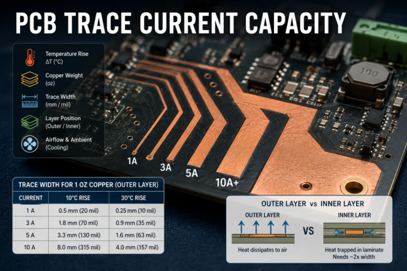
- Trace Widths: Reduce copper trace widths to minimize space consumption while routing interconnections. Careful consideration of resistance and current capacity effects is necessary, with traces under 0.2mm often used for high-density boards.
- Manual Layout: While autorouters can provide initial routing arrangements, achieving the most space-efficient PCBs often requires the expertise of a layout designer who can manually optimize trace paths for maximum efficiency.
- Layer Stackups: Increasing the number of layers in a PCB provides greater routing flexibility and allows for more compact layouts. However, keep in mind that each additional layer comes with increased manufacturing costs.
- 3D Construction: Innovative rigid-flex PCB technology enables the creation of 3D PCB shapes by folding 2D boards. While this approach comes with added costs, it can significantly increase functional density and enable compact enclosures when carefully planned.
Benefits of Smaller Printed Circuit Boards
Reducing the dimensions of printed circuit boards within functional limits offers several advantages:
- More Compact Products: Smaller PCBs enable the design of more portable and compact consumer gadgets, which is particularly important for mobile devices like smartphones. Compact PCBs also save space in instruments and other electronic devices.
- Lower Materials Cost: Smaller PCBs require less substrate material and copper foil during fabrication, resulting in cost savings on materials. Fewer layers and shorter trace lengths further contribute to reduced material costs.
- Better Signal Integrity: Shorter trace lengths on miniaturized PCBs lead to reduced interference and signal distortion, facilitating cleaner and faster high-speed signal transmission. This is crucial for ensuring the quality performance of electronic devices.
- Simplified Assembly: Smaller PCBs are easier to assemble, both manually and through automated processes. Hand soldering becomes more manageable, and automated assembly is faster and more efficient with reduced board sizes.
Challenges with Miniaturized PCBs
While miniaturizing PCBs offers numerous benefits, it also presents certain challenges that engineers must address:
- Complex Routing: Reducing board dimensions significantly increases the complexity of routing densely packed components with limited space. This often requires additional layers or the expertise of skilled layout engineers to ensure successful interconnections.
- Thermal Issues: Concentrating heat generation into a smaller PCB area poses challenges for thermal management. Careful engineering, including the use of ground planes, thermal vias, heat sinks, and airflow management, is essential to prevent overheating.
- Assembly Difficulty: The extremely small components and tight spacings on compact PCBs make hand soldering and assembly more challenging, leading to increased difficulty and potential errors. Reworking faulty solder joints becomes especially daunting on a smaller scale.
- High-Frequency Losses: Excessive reduction of trace lengths can paradoxically increase resistive signal losses at microwave frequencies beyond a few gigahertz. This limitation can impact miniaturization efforts for high-frequency radio applications.
Conclusion
The optimization and reduction of PCB size have become critical considerations in the world of electronics. As demands for compactness continue to rise, engineers must leverage strategies like careful component selection, manual layout optimization, multilayer stackups, advanced routing techniques, and 3D integration when necessary to meet size constraints.
Custom dimensions tailored to specific applications and pushing the limits of standard PCB sizes offer distinct advantages over one-size-fits-all approaches. While miniaturized PCBs offer benefits such as compact product design, lower materials costs, improved signal integrity, and simplified assembly, they also come with challenges related to complex routing, thermal management, assembly difficulty, and high-frequency losses.
Ultimately, achieving the right-sized PCBs involves striking a balance between cost, performance, and manufacturability trade-offs. By embracing innovative design practices and staying abreast of technological advancements, engineers can continue to meet the growing demand for miniaturization in electronic devices.
FAQ
Does reducing PCB size always increase its cost?
Not necessarily. While in some cases, reducing size may increase costs (e.g., due to adding more layers or using smaller components), in many cases, a well-optimized design can actually reduce costs. Efficient design and optimization (such as reducing material waste and simplifying manufacturing) can lower costs significantly. Therefore, the cost of a PCB is closely related to the design choices.
How can I balance size reduction with cost increases in PCB design?
When designing a PCB, choosing the right number of layers, component layout, component types, and routing strategies can help reduce size while controlling costs. Optimizing the design to avoid unnecessary complexity and excessive material use can achieve cost savings.
How does reducing PCB size improve signal integrity?
Smaller PCBs typically shorten trace lengths, which helps reduce signal interference and distortion, thus improving signal integrity. However, for high-frequency applications, particular attention must be given to impedance matching and signal loss to ensure performance.
What are the thermal management challenges in miniaturized PCBs?
In smaller PCBs, heat tends to concentrate, making thermal management a significant challenge. Effective thermal management can be achieved by using thermal vias, heat sinks, ground planes, and proper component placement. The design should carefully consider how to manage heat flow to prevent overheating.
Are miniaturized PCBs suitable for high-frequency applications?
Miniaturization can increase signal loss at higher frequencies, particularly above several gigahertz. Therefore, when designing for high-frequency applications, it’s essential to focus on minimizing signal loss and optimizing signal paths to ensure performance.
How does 3D PCB technology help in reducing size?
3D PCB technology allows for folding 2D boards into three-dimensional shapes, significantly increasing functional density and reducing the overall size. While this approach may add some costs, it provides an effective solution for compact designs in limited spaces.

Recommended Posts

PCB Current Calculator: Sizing Trace Width and Vias with the IPC-2221 Formula
Figure 1. Pcb Current Calculator reference image for PCB...

Microphone PCB Design: How the Board Itself Shapes Your Audio Quality
Figure 1. Microphone Pcb reference image for PCB...

Board-to-Board Connector: Types, Specifications, and How to Select One
Figure 1. Board To Board Connector reference image for PCB...
PCB Trace Width Calculator: How to Size Traces for Current, Voltage Drop, and Impedance
Figure 1. A PCB trace width calculator is a starting point...
How to get a quote for PCBs
Let us run DFM/DFA analysis for you and get back to you with a report.
You can upload your files securely through our website.
We require the following information in order to give you a quote:
-
- Gerber, ODB++, or .pcb, spec.
- BOM list if you require assembly
- Quantity
- Turn time
In addition to PCB manufacturing, we offer a comprehensive range of electronic services, including PCB design, PCBA (Printed Circuit Board Assembly), and turnkey solutions. Whether you need help with prototyping, design verification, component sourcing, or mass production, we provide end-to-end support to ensure your project’s success. For PCBA services, please provide your BOM (Bill of Materials) and any specific assembly instructions. We also offer DFM/DFA analysis to optimize your designs for manufacturability and assembly, ensuring a smooth production process.