
Ceramic PCB Via and Metallization: Technical Guide

Introduction: Via Structures in Ceramic PCBs
Via structures in ceramic PCBs serve two critical functions: establishing electrical interconnection between circuit layers and providing efficient thermal conduction pathways from heat-generating components to heat sinks. Unlike traditional FR-4 boards, ceramic substrates composed of alumina (Al₂O₃), aluminum nitride (AlN), or silicon nitride (Si₃N₄) are inherently non-conductive materials.
This fundamental characteristic means that via and metallization in ceramic PCBs must rely entirely on specialized metal deposition and filling processes to create reliable interlayer connections. The quality of these metallized via structures directly determines both the electrical performance and thermal management capability of the finished assembly.
Ceramic PCB Via Types and Configurations
Understanding the various ceramic PCB via configurations enables designers to optimize circuit performance for specific applications. Each via type offers distinct advantages in terms of signal routing flexibility, thermal performance, and manufacturing complexity.
Through-Hole Vias
Through-hole vias penetrate the entire thickness of the ceramic substrate, creating a continuous conductive path from top to bottom surface. These structures provide excellent current-carrying capacity for both signal transmission and thermal dissipation. The relatively large cross-sectional area of through-hole configurations delivers lower electrical resistance and higher thermal conductivity compared to smaller via geometries.
Blind and Buried Vias
Blind vias extend from an outer layer into internal layers without penetrating the entire substrate, while buried vias exist entirely within internal layers. These advanced ceramic PCB via structures enable higher circuit density by freeing up surface area. Key advantages include:
- Space optimization – Surface area remains available for additional component placement and routing.
- Signal integrity – Reduced stub effects minimize electromagnetic interference between circuit layers.
- High-density capability – Critical for RF modules, sensor arrays, and miniaturized assemblies.
Manufacturing complexity increases with these structures, requiring precise layer alignment during fabrication.
Filled Vias
Filled ceramic PCB via configurations incorporate conductive materials such as copper, silver, tungsten, or molybdenum within the via barrel. This eliminates the hollow center of plated-only vias, significantly improving thermal conductivity and structural integrity. Applications demanding maximum heat dissipation, such as LED modules and power electronics, typically specify filled thermal vias to create efficient heat transfer pathways through the substrate.

Thick Film Ceramic PCBs
Metallization Techniques for Ceramic PCB Vias
The metallization process determines the adhesion strength, electrical conductivity, and long-term reliability of ceramic PCB via structures. Different techniques suit different substrate materials and application requirements.
Thick-Film Metallization
Thick-film metallization involves screen-printing conductive pastes containing metal particles onto the ceramic surface, followed by high-temperature sintering. Silver and tungsten pastes represent the most common materials, with silver offering excellent conductivity and tungsten providing superior adhesion to alumina substrates. This approach creates conductor layers typically ranging from 10 to 25 micrometers thickness.
The process accommodates ceramic PCB via filling by printing paste into pre-formed holes before sintering. Feature resolution limits this technique to circuits with line widths above 100 micrometers.
Thin-Film Metallization
Thin-film processes employ vacuum deposition techniques such as sputtering or evaporation to create metallization layers below 5 micrometers thickness. These methods enable fine-line circuitry with features down to 20 micrometers, ideal for high-frequency applications and miniaturized substrates.
The thin-film approach to ceramic PCB via formation typically combines sputter deposition for seed layer creation, photolithographic patterning, and electroplating for thickness buildup. This achieves excellent dimensional control for complex multilayer structures.
Direct Copper Bonding and Active Metal Brazing
Direct copper bonding (DCB) creates a metallurgical bond between copper foil and ceramic substrates through high-temperature oxidation, producing exceptional adhesion strength. The process creates copper layers typically 0.3 to 0.8 millimeters thick that handle high current loads. Active metal brazing (AMB) employs reactive metals such as titanium to promote chemical bonding between copper and ceramic surfaces.
These techniques provide robust metallization for power modules but require careful thermal management due to coefficient of thermal expansion mismatch. Integration with ceramic PCB via structures typically occurs through subsequent drilling and electroplating.
Electroplating for Via Metallization
Electroless plating followed by electrolytic plating represents the standard method for metallizing via walls in ceramic substrates. The electroless deposition creates a thin conductive seed layer through chemical reduction, enabling subsequent electrolytic buildup to the desired copper thickness. This ceramic PCB via metallization sequence achieves uniform coverage even in high-aspect-ratio holes.
The process requires careful surface preparation including cleaning and activation steps to ensure proper adhesion. Plating chemistry must be optimized for the specific ceramic material to prevent voids or delamination.

Thin Film Ceramic PCBs
Via Filling and Ceramic PCB Reliability
The long-term reliability of ceramic PCB via structures depends critically on filling materials, process control, and design optimization to manage stress between dissimilar materials.
Filling Materials and Methods
Material selection for ceramic PCB via filling balances electrical performance, thermal conductivity, and coefficient of thermal expansion matching:
- Copper filling – Highest electrical and thermal conductivity but requires oxidation prevention during high-temperature operations.
- Silver paste – Good compatibility with thick-film processing for moderate thermal requirements.
- Tungsten and molybdenum – Thermal expansion coefficients closer to ceramics reduce stress but accept lower conductivity.
Vacuum-assisted sintering and sequential electroplating represent the most reliable approaches for creating void-free structures that maintain integrity through thermal cycling.
Thermal Expansion Mismatch
The coefficient of thermal expansion difference between ceramic substrates and metallic via filling creates mechanical stress during temperature excursions. Alumina exhibits thermal expansion around 7 ppm/°C, while copper expands at approximately 17 ppm/°C, creating significant stress at ceramic-metal interfaces.
Mitigation strategies include selecting filling materials with coefficients closer to the substrate, controlling via geometry to minimize stress concentration, and incorporating stress-relief features in metallization design. Testing protocols should include thermal cycling between temperature extremes representative of the intended application environment.
Reliability Testing and Failure Modes
Comprehensive reliability assessment for ceramic PCB via structures combines electrical testing, thermal cycling, mechanical stress testing, and non-destructive inspection. Typical failure modes include:
- Electrical opens – Crack propagation through the via barrel interrupts current flow.
- Increased resistance – Void formation or metal migration degrades electrical performance.
- Intermittent connections – Thermal fatigue at material interfaces causes contact reliability issues.
Cross-sectional microscopy reveals internal defects while X-ray imaging enables non-destructive inspection of via filling quality. Design validation should include temperature cycling from -55°C to +150°C or higher depending on application requirements.

Ceramic PCB Manufacturer
Design and Process Optimization for Ceramic PCB Vias
Strategic design choices and manufacturing process refinement maximize ceramic PCB via performance while maintaining cost-effectiveness and manufacturability.
Via Distribution and Thermal Path Design
Optimizing via placement relative to heat-generating components creates efficient thermal conduction pathways that minimize junction temperatures. High-power components benefit from arrays of thermal vias positioned directly beneath the device footprint to spread heat into larger copper areas or external heat sinks.
Via pitch and diameter should balance thermal performance against mechanical reliability, with aspect ratios typically maintained below 10:1 for conventional plating processes. Dense via arrays under power semiconductors significantly reduce thermal resistance.
Manufacturing Considerations
Process capability limits impose practical constraints on ceramic PCB via design parameters. Minimum via diameters typically range from 0.15 to 0.30 millimeters depending on substrate thickness and drilling method, with laser drilling enabling smaller features than mechanical drilling.
Metallization thickness requirements depend on current-carrying capacity and must account for reduced plating thickness at via centers compared to entrance regions. Manufacturers should establish process control methods including via resistance measurement, metallization cross-section analysis, and thermal impedance testing.
Partnering with a Capable Ceramic PCB Manufacturer
Achieving reliable ceramic PCB via structures requires specialized equipment, process expertise, and quality control systems that only experienced manufacturers possess. The complex interaction between substrate material properties, metallization chemistry, and thermal processing demands deep technical knowledge accumulated through production experience.
Manufacturing facilities must maintain capability for precision drilling or laser ablation, multiple metallization techniques including thick-film and thin-film processes, controlled atmosphere sintering, and electroplating with precise thickness control.
Highleap Electronics brings comprehensive ceramic substrate fabrication capabilities including advanced via formation, metallization, and filling processes developed through extensive work with alumina, aluminum nitride, and silicon nitride materials. Our engineering team provides design for manufacturability analysis to optimize via configurations for both performance and production yield. We invite you to submit your design files for a detailed feasibility assessment and process recommendation tailored to your specific application requirements.

Recommended Posts
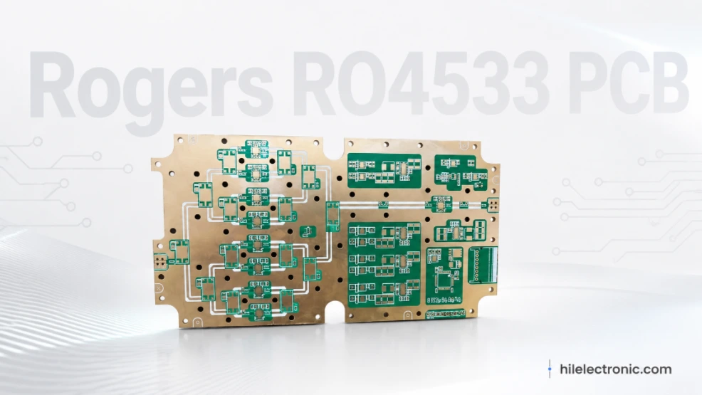
Rogers RO4533 PCB Manufacturing for Cost-Sensitive RF Products
RO4533 should be handled as a grade-specific commercial RF...
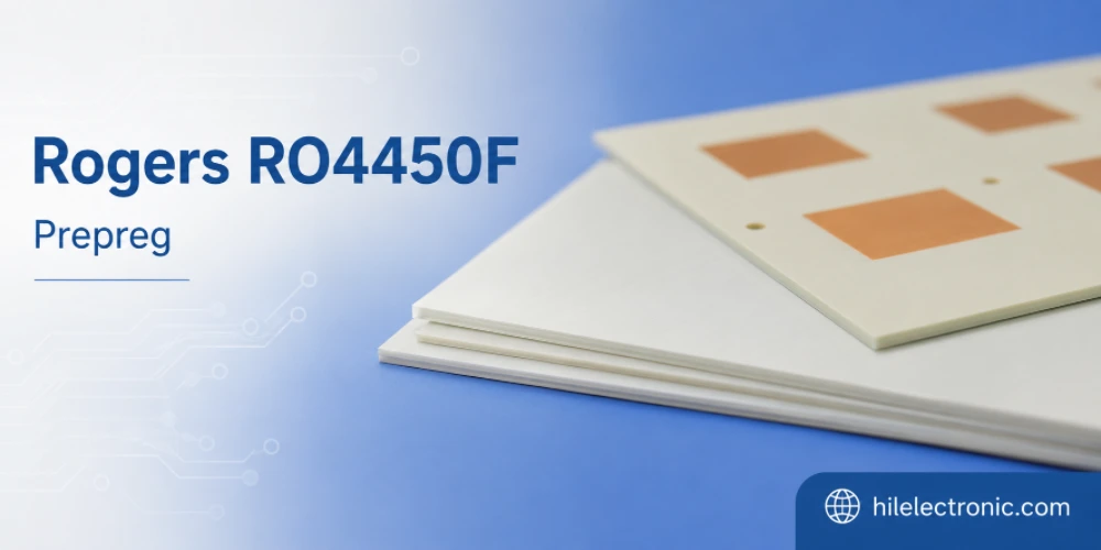
Rogers RO4450F Prepreg for Multilayer RF PCB Manufacturing
“RO4450F prepreg” is not enough information to manufacture...
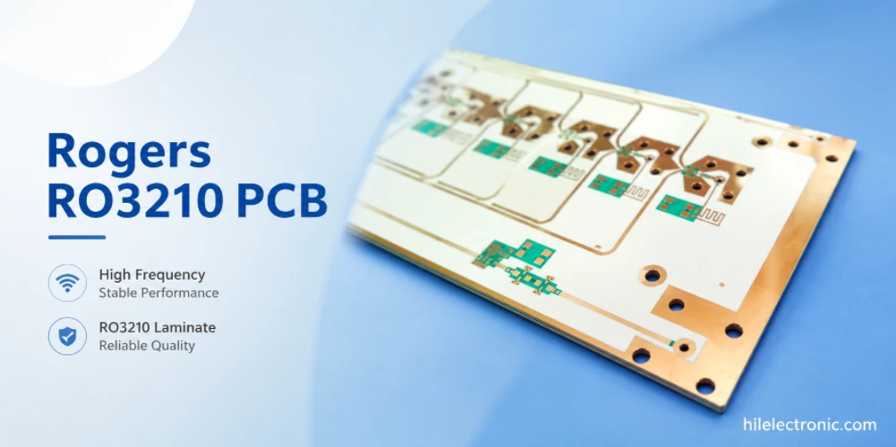
Rogers RO3210 PCB Manufacturing for Extremely Compact RF Circuits
RO3210 is not a routine material upgrade. Rogers publishes...
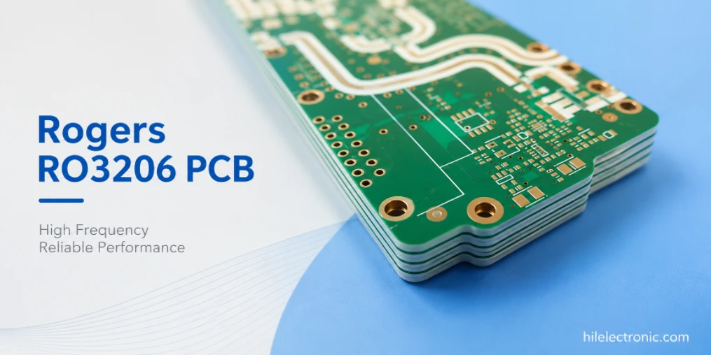
Rogers RO3206 PCB Manufacturing for Miniaturized RF Products
An RO3206 quotation should begin with the dimensions the...
How to get a quote for PCBs
Let‘s run DFM/DFA analysis for you and get back to you with a report. You can upload your files securely through our website. We require the following information in order to give you a quote:
-
- Gerber, ODB++, or .pcb, spec.
- BOM list if you require assembly
- Quantity
- Turn time
In addition to PCB manufacturing, we offer a comprehensive range of electronic services, including PCB design, PCBA, and turnkey solutions. Whether you need help with prototyping, design verification, component sourcing, or mass production, we provide end-to-end support to ensure your project’s success.
For PCBA services, please provide your BOM (Bill of Materials) and any specific assembly instructions. We also offer DFM/DFA analysis to optimize your designs for manufacturability and assembly, ensuring a smooth production process.