
Electronic Keyboard PCB Manufacturing & Assembly | Highleap

The electronic keyboard represents one of the most sophisticated examples of human-machine interface engineering in consumer electronics. From professional synthesizers to digital pianos, these instruments demand exceptional precision in their printed circuit board (PCB) design and manufacturing processes. As the foundation of every electronic keyboard’s functionality, the PCB architecture directly influences instrument performance, reliability, and user experience.
At Highleap Electronics, our extensive experience in PCB manufacturing and assembly for electronic keyboards has provided unique insights into the technical challenges and manufacturing considerations that define this specialized market segment. This comprehensive analysis examines the critical aspects of electronic keyboard PCB development, from initial design considerations through final assembly optimization.
Circuit Architecture Design Principles for Electronic Keyboard Applications
Multi-Layer PCB Configuration Analysis
Electronic keyboard PCBs typically employ sophisticated multi-layer architectures to accommodate the complex signal routing requirements inherent in modern digital music instruments. The standard configuration utilizes a minimum of four layers, with professional-grade keyboards often requiring six to eight layers to manage the intricate signal pathways effectively.
Layer Stack-Up Configuration:
- Layer 1: Component placement and primary signal routing
- Layer 2: Ground plane for noise reduction and EMI shielding
- Layer 3: Power distribution network (PDN) optimization
- Layer 4: Secondary signal routing and return paths
- Layers 5-8: Specialized routing for high-speed digital signals and analog audio pathways
The impedance control requirements for electronic keyboard PCBs are particularly stringent, with differential pair impedances typically maintained at 100Ω ±10% for USB and MIDI interfaces, while single-ended traces require 50Ω ±10% characteristic impedance for optimal signal integrity.
Signal Integrity Considerations
Electronic keyboards process multiple signal types simultaneously, including low-frequency control voltages, high-frequency digital data, and sensitive analog audio signals. The PCB design must implement robust isolation techniques to prevent cross-talk and maintain signal fidelity across all operational frequencies.
Critical design parameters include:
- Minimum trace spacing of 0.2mm for high-density routing
- Via stitching density of minimum 1 via per 5mm for layer transitions
- Copper pour strategies for thermal management and noise reduction
- Strategic component placement to minimize loop areas and reduce EMI
PCB Manufacturing and Assembly Services Tailored for Electronic Keyboard Applications
Highleap Electronics specializes in high-precision PCB fabrication and advanced PCB assembly, supporting global brands in the electronic keyboard and music technology industries. Whether it’s a digital piano mainboard or a synthesizer control interface, we provide reliable, scalable solutions from prototype to mass production.
Our core capabilities include:
- Multi-layer PCB fabrication with impedance control for audio-digital systems
- SMT and through-hole assembly for diverse component requirements
- Cleanroom soldering environments for sensitive analog signal paths
- Comprehensive testing including AOI, X-ray, and functional tests
We understand the unique electrical, acoustic, and mechanical requirements of electronic musical instruments and deliver production consistency at every scale. With full ISO 9001:2015 compliance and strong supply chain management, we help you bring high-performance keyboards to market—faster and more reliably.
Manufacturing Process Optimization for Electronic Keyboard PCBs
Advanced Fabrication Techniques
The manufacturing of electronic keyboard PCBs requires precise control over multiple fabrication parameters to ensure consistent performance across production volumes. Our manufacturing process incorporates several advanced techniques specifically optimized for the unique requirements of musical instrument electronics.
Critical Process Parameters:
| Parameter | Specification | Tolerance |
|---|---|---|
| Copper Thickness | 1oz (35μm) standard, 2oz (70μm) for power layers | ±10% |
| Via Hole Size | 0.2mm minimum diameter | ±0.05mm |
| Trace Width | 0.1mm minimum | ±0.025mm |
| Solder Mask Registration | Green/Black standard | ±0.075mm |
| Surface Finish | HASL/ENIG/OSP | Per IPC-A-600 Class 2 |
The fabrication process utilizes controlled impedance manufacturing with continuous monitoring to ensure electrical performance specifications are maintained throughout production. Automated optical inspection (AOI) systems verify trace geometry and via formation at multiple process stages.
Quality Assurance Protocols
Electronic keyboard PCB manufacturing demands rigorous quality control measures due to the performance-critical nature of musical instrument applications. End-users expect consistent, reliable operation across extended operational periods, often in challenging environmental conditions.
Our quality assurance framework encompasses:
- Incoming Material Inspection: Comprehensive testing of substrate materials, copper foils, and chemical processes
- In-Process Monitoring: Real-time parameter tracking during etching, plating, and drilling operations
- Electrical Testing: 100% continuity and isolation testing using flying probe technology
- Functional Verification: Sample-based testing of completed assemblies under simulated operational conditions

Component Assembly Methodologies for Electronic Keyboard Systems
Electronic keyboard assembly presents unique challenges due to the diverse component types and varying thermal profiles required for optimal solder joint formation. The assembly process must accommodate everything from precision potentiometers and mechanical switches to high-pin-count microprocessors and specialized audio processing integrated circuits.
Surface Mount Technology (SMT) Assembly Process
The SMT assembly process for electronic keyboards follows a carefully optimized sequence designed to minimize thermal stress while ensuring reliable solder joint formation across all component types. The process utilizes a combination of selective and reflow soldering techniques to accommodate components with varying thermal sensitivities.
Reflow Profile Optimization:
- Pre-heat zone: 150–180°C at 2–3°C/second ramp rate
- Thermal soak: 180–200°C maintained for 60–90 seconds
- Reflow peak: 235–245°C for lead-free alloys (SAC305)
- Cooling phase: <6°C/second to prevent thermal shock
The assembly sequence prioritizes component placement based on thermal mass and sensitivity, with precision components such as crystal oscillators and analog reference circuits placed first to minimize exposure to multiple thermal cycles.
Through-Hole Component Integration
Electronic keyboards typically incorporate numerous through-hole components including mechanical switches, potentiometers, jacks, and connectors that require selective soldering techniques. The integration of these components with the SMT assembly process requires careful coordination to maintain joint quality and prevent thermal damage.
Selective Soldering Parameters:
- Flux application: Spray or wave application with no-clean chemistry
- Pre-heat temperature: 100–120°C substrate temperature
- Solder pot temperature: 270–280°C for Sn/Pb alloys
- Contact time: 2–4 seconds depending on joint thermal mass
- Nitrogen atmosphere: <100ppm oxygen for optimal wetting
Electromagnetic Compatibility (EMC) Design Considerations
Electronic keyboards must comply with stringent electromagnetic compatibility requirements due to their audio signal processing capabilities and potential interference with other electronic equipment. The PCB design and assembly process must incorporate specific EMC mitigation strategies to ensure regulatory compliance and optimal performance.
Noise Reduction Strategies
The multi-domain signal environment within electronic keyboards creates unique EMC challenges that require comprehensive design approaches. Digital switching noise from microprocessors and DSP circuits can interfere with sensitive analog audio circuits, while external electromagnetic interference can affect both digital control systems and audio signal quality.
Primary EMC Mitigation Techniques:
- Power Distribution Network (PDN) Optimization: Implementation of distributed decoupling capacitor networks with values ranging from 100pF to 1000μF placed strategically throughout the PCB layout
- Ground Plane Segmentation: Careful separation of analog and digital ground domains with single-point connection strategies to minimize ground loop formation
- Shielding Implementation: Strategic placement of EMI shields over high-frequency circuits and sensitive analog sections
- Filter Integration: Incorporation of common-mode and differential-mode filters at interface connections
Regulatory Compliance Framework
Electronic keyboard products must demonstrate compliance with multiple international EMC standards including FCC Part 15 (United States), EN 55032 (Europe), and VCCI (Japan). The PCB design and assembly process must ensure consistent performance across all applicable frequency ranges and operational conditions.
Testing protocols include radiated emissions measurements from 30MHz to 1GHz, conducted emissions testing from 150kHz to 30MHz, and immunity testing across multiple interference scenarios. Pre-compliance testing during the development phase identifies potential issues before final certification testing.
Conclusion
Electronic keyboards demand precise, reliable, and acoustically optimized electronic systems—and at Highleap Electronics, we deliver PCB and PCBA solutions that meet the unique technical standards of modern musical instruments.
Our experience with high-density layouts, analog-digital signal integrity, and rigorous testing ensures that keyboard manufacturers receive consistent, high-performance electronic assemblies ready for demanding musical applications.
While electronic keyboards represent one of many advanced applications we support, our core strength lies in delivering scalable, high-quality PCB and PCBA manufacturing across diverse industries—from audio and automotive to industrial and medical electronics.
Why leading brands trust Highleap:
- Expert handling of analog + digital hybrid circuits
- Precision SMT assembly under ISO-certified processes
- 100% electrical testing and visual inspection
- Scalable production from prototype to full-volume builds
Whether you’re building the next generation of musical instruments or any other advanced electronic device, Highleap Electronics is your proven partner in performance and quality.

Recommended Posts

PCB Copper Plating: Process, Thickness, Quality Control
Figure 1. PCB copper plating process for hole-wall and...
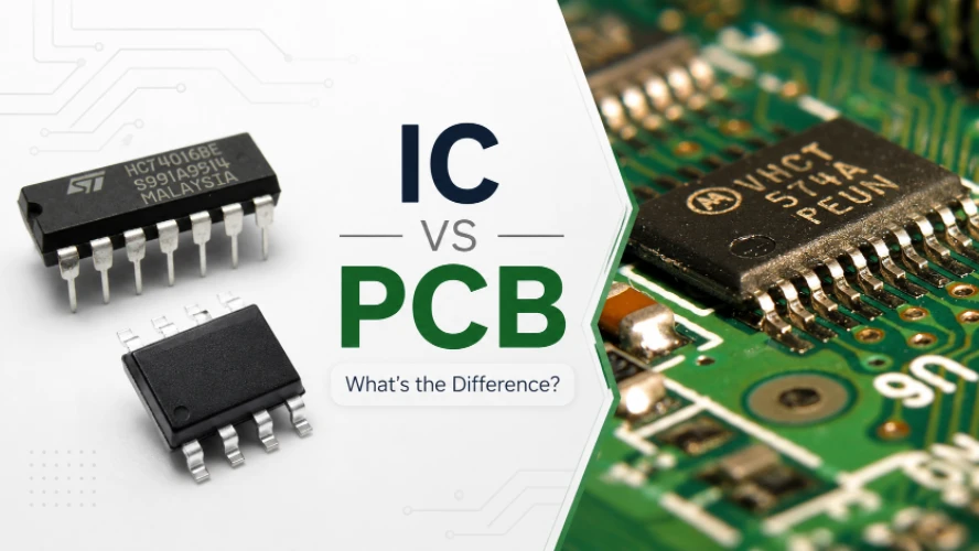
IC vs PCB: What’s the Difference and How They Work Together
Figure 1. IC vs PCB comparison showing the chip and the...

Electronic Reverse Engineering Service
You send us a physical PCB — or an electronic product...

High Frequency PCB Manufacturer China Selection Guide
Table of Contents China's HF PCB Manufacturing Capability...
How to get a quote for PCBs
Let‘s run DFM/DFA analysis for you and get back to you with a report. You can upload your files securely through our website. We require the following information in order to give you a quote:
-
- Gerber, ODB++, or .pcb, spec.
- BOM list if you require assembly
- Quantity
- Turn time
In addition to PCB manufacturing, we offer a comprehensive range of electronic services, including PCB design, PCBA, and turnkey solutions. Whether you need help with prototyping, design verification, component sourcing, or mass production, we provide end-to-end support to ensure your project’s success.
For PCBA services, please provide your BOM (Bill of Materials) and any specific assembly instructions. We also offer DFM/DFA analysis to optimize your designs for manufacturability and assembly, ensuring a smooth production process.