
Electronic Product Development with PCB Manufacturing

Electronic product development has become increasingly complex as the demand for higher performance in smaller form factors grows. For many companies, integrating sophisticated PCB manufacturing and assembly expertise is crucial to success. Strategic manufacturing partnerships, forged early in the development process, can be the difference between market success and failure.
The development of modern electronic products, especially those that operate at gigahertz frequencies, requires advanced PCB technologies and specialized materials. Companies need to understand how manufacturing impacts design feasibility, costs, and time-to-market in order to achieve success.
Why PCB Manufacturing is Critical to Electronic Product Development
When it comes to electronic product development, the ability to effectively balance manufacturing feasibility with ambitious design goals is crucial. Designs that operate above 1 GHz require precise controlled impedance tolerances (±5 ohms), trace widths approaching 75 micrometers, and the use of specialized low-loss laminates. Can your current manufacturing methods meet these demands?
Signal integrity preservation is critical for high-frequency designs and requires meticulous dielectric thickness control and copper surface roughness management. Advanced PCB manufacturing capabilities, such as Class 6 PCB fabrication, are necessary to meet these specifications consistently.
Thermal management also plays a crucial role, particularly for power densities exceeding 10 watts per square inch. Achieving efficient thermal management requires strategic copper plane placement and precise thermal via implementation, both of which are dependent on the manufacturing process.
The Risks of Inadequate PCB Manufacturing Support
Without the support of professional PCB manufacturers, organizations face the risks of yield issues, performance degradation, and cost overruns that compromise the project’s viability. Manufacturing is the foundation that translates design specifications into tangible products. Inadequate PCB manufacturing support often leads to delays and costly revisions, undermining the potential for market success.
By partnering with experienced PCB manufacturers, electronic product developers ensure that designs are manufacturable, minimizing errors and maximizing performance. The collaboration between design teams and manufacturers enables the seamless transition from concept to product, keeping the project on track for success.
Assembly Challenges and Solutions in Modern Electronic Product Development
As electronic products become more compact, powerful, and multifunctional, PCB assembly evolves into a complex engineering process that must be considered from the very beginning of product development. Treating assembly as a design-driven discipline—not just a production step—helps prevent costly mistakes and enables smoother scaling from prototype to mass production.
This page covers the development workflow from prototype files to production transfer. If the immediate issue is early cost planning, use budgetary quotes for product development; for first articles and engineering samples, review prototype PCB manufacturing.
Precision Placement of Fine-Pitch Components
Modern assemblies often include fine-pitch BGA, QFN, or CSP packages. These components require sub-micron placement accuracy and highly controlled reflow environments. Small variances in solder paste, stencil thickness, or PCB flatness can lead to:
- Misalignment or floating components
- Tombstoning of 0201/01005 passives
- PCB warpage in thin or high-layer-count designs
Best practices include:
- Using vision-guided placement machines with ±25μm accuracy
- Optimizing stencil design and paste selection for rheological stability
- Running DFM checks early to identify layout-related risks
Mixed-Technology Integration Challenges
Today’s designs often combine SMT, MEMS sensors, flex circuits, RF modules, and optical components. These demand precise handling and tailored soldering strategies.
Common issues include:
- Damage from repeated reflow cycles
- Height variation causing solder inconsistencies
- Manual placement reducing yield and repeatability
Solutions:
- Use staggered or selective soldering for sensitive parts
- Collaborate with EMS providers during component selection
- Apply nitrogen-assisted reflow for precision and thermal protection
Supply Chain Disruption and Component Substitution
Electronic component shortages and obsolescence can derail production timelines—especially after BOMs are finalized.
Challenges:
- Lead times of 30–52 weeks for core ICs or capacitors
- Risk of incompatible alternates or unverified substitutes
- Quality and counterfeit issues from non-authorized sources
Proactive strategies:
- Define AVL (Approved Vendor List) with validated alternates
- Prioritize automotive or industrial-grade component lines
- Work with EMS partners who offer inventory forecasts and risk alerts
Inspection and Quality Validation Beyond Visual Checks
As assembly density increases, visual inspection is no longer sufficient. BGA and hidden-joint packages require advanced inspection and testing.
Typical failure risks:
- Solder voids or bridges undetectable without X-ray
- Cold/cracked joints causing intermittent field failures
- Inadequate test coverage due to missing fixtures or plans
Recommended tools and approaches:
- AOI (Automated Optical Inspection)
- X-ray imaging for hidden solder joints
- ICT and FCT for connectivity and full-system validation
- SPC and traceable QA reports to ensure process stability
Why Assembly Must Start with Design Thinking
Assembly decisions directly affect layout rules, part choices, thermal behavior, and testability. Treating assembly as an engineering task—not just factory work—unlocks:
- Higher product reliability
- Faster development cycles
- Lower rework and field failure rates
- Streamlined transition from prototype to full-scale production
Collaboration Between Design and Manufacturing in Electronic Product Development
In traditional electronic product development workflows, there is often a disconnect between design engineering and manufacturing execution. Design teams focus on performance optimization—pushing for faster processors, higher power densities, and tighter form factors—while manufacturing teams prioritize yield, cost control, and process repeatability. This misalignment can result in delayed product launches, increased development costs, and compromised product reliability.
Modern hardware development demands a more integrated approach. Leading electronics companies now embed manufacturing considerations into the early stages of product design. Close collaboration with PCB fabrication and assembly partners during the design phase ensures that electrical, thermal, and mechanical requirements are balanced with manufacturability. This early alignment reduces redesign cycles and enables faster prototyping, especially for high-speed digital, RF, or power electronics products.
One of the most critical examples is thermal management. In compact IoT devices, power converters, or edge computing hardware, high heat loads require strategic coordination between PCB layout, component placement, copper plane design, and enclosure-level heat dissipation. Effective thermal performance depends not only on simulation, but also on real-world manufacturing processes, including thermal interface material application, reflow profile control, and heatsink integration.
Ultimately, the gap between design intent and manufacturing feasibility can be closed by fostering early and continuous communication between engineering and production teams. By partnering with experienced EMS providers and PCB manufacturers who understand the nuances of electronic product lifecycle management, development teams can achieve faster time to market, improved reliability, and reduced total cost of ownership.

Mechanical Integration Requirements in Electronic Product Development
Why Mechanical Integration Matters in Electronic Product Development
Mechanical design choices directly influence whether an electronic product can survive its operating environment and reach the market on time. Tight form factors, thermal constraints, and regulatory tests all converge at the enclosure. If mechanical integration is treated as an after-thought, late-stage redesigns become inevitable and expensive.
Meeting Environmental and Sealing Standards
Many electronic product development programs must satisfy IP67 or higher ingress-protection ratings. Achieving this reliably in volume production requires precise gasket compression control, uniform surface finishes, and repeatable torque or ultrasonic-weld processes. At the same time, electromagnetic compatibility targets often call for shielding effectiveness above 80 dB up to 18 GHz. This drives decisions on conductive gaskets, plated plastics, or multi-metal hybrid housings—none of which can be validated by enclosure design alone; they must be co-engineered with PCB stack-ups and ground-plane strategy.
Coordinating PCB, Assembly, and Enclosure Design
Successful mechanical integration extends beyond individual parts: cable routing, connector access for test fixtures, and the sequence in which boards slide, fold, or screw into the chassis all affect yield. A millimetre saved on board outline may demand a costlier rigid-flex, while an extra fastening step could double takt time on the line. Bringing mechanical, electrical, and assembly engineers to the same table early ensures thermal pads align with heat-spreading copper, RF shields clear standoffs, and screw bosses do not shadow critical traces.
Leveraging Unified Manufacturing Partnerships
Projects that treat enclosure fabrication, PCB manufacturing, and system assembly as separate silos often struggle with tolerance stack-ups and last-minute design changes. By engaging a unified manufacturing partner—one that owns or tightly coordinates all three disciplines—teams gain a single source of DFM input, tooling feedback, and pilot-run data. This end-to-end visibility shortens debug loops, locks down environmental compliance sooner, and ultimately delivers more robust electronic products to market.
Strategic Partnership with Highleap Electronics
Highleap Electronics offers integrated PCB manufacturing and assembly services tailored for complex electronic product development. From high-density interconnects to controlled impedance processing and advanced material handling, our capabilities are designed to support high-performance, high-reliability hardware.
In addition to manufacturing, we provide support across sourcing, quality control, and supply chain planning—helping reduce risk and improve cost predictability. Our engineering team works closely with yours to ensure smooth transitions from design to production.
By partnering early with Highleap, you gain more than a supplier—you gain a technical partner committed to your product’s success.

Recommended Posts

PCB Copper Plating: Process, Thickness, Quality Control
Figure 1. PCB copper plating process for hole-wall and...
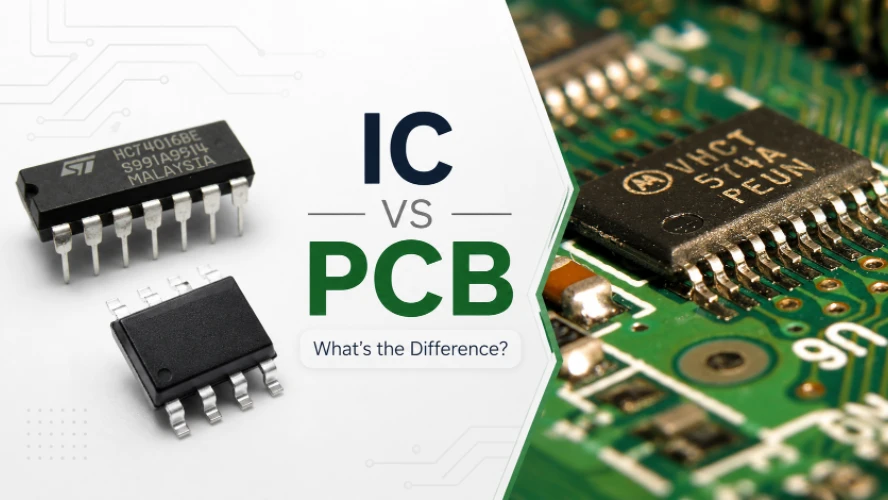
IC vs PCB: What’s the Difference and How They Work Together
Figure 1. IC vs PCB comparison showing the chip and the...

Electronic Reverse Engineering Service
You send us a physical PCB — or an electronic product...

High Frequency PCB Manufacturer China Selection Guide
Table of Contents China's HF PCB Manufacturing Capability...
How to get a quote for PCBs
Let‘s run DFM/DFA analysis for you and get back to you with a report. You can upload your files securely through our website. We require the following information in order to give you a quote:
-
- Gerber, ODB++, or .pcb, spec.
- BOM list if you require assembly
- Quantity
- Turn time
In addition to PCB manufacturing, we offer a comprehensive range of electronic services, including PCB design, PCBA, and turnkey solutions. Whether you need help with prototyping, design verification, component sourcing, or mass production, we provide end-to-end support to ensure your project’s success.
For PCBA services, please provide your BOM (Bill of Materials) and any specific assembly instructions. We also offer DFM/DFA analysis to optimize your designs for manufacturability and assembly, ensuring a smooth production process.