
HDI PCB Cost Drivers & Optimization Strategies

Understanding HDI PCB cost is essential for electronics manufacturers seeking to balance performance with budget constraints. This article examines the primary factors that drive HDI PCB cost and presents actionable optimization strategies across design and manufacturing stages. By addressing cost drivers systematically, engineering teams can reduce expenses without compromising signal integrity or reliability requirements.
Understanding HDI PCB Cost Structure
HDI PCB cost analysis requires a comprehensive view of the entire production value chain. Cost structure typically divides into material procurement, manufacturing processes, quality assurance testing, and surface finishing operations. Each component contributes differently to the total HDI PCB cost, with material and manufacturing processes accounting for the largest portions.
Material costs encompass copper-clad laminates, prepreg layers, copper foil thickness specifications, and tolerance grade selections. Manufacturing process costs include sequential lamination cycles, laser drilling operations, copper plating, and electroplating procedures. Testing and yield considerations introduce additional expenses through flying probe testing and reliability validation protocols. Surface finish options such as ENIG, OSP, or immersion silver further impact the final HDI PCB cost structure.
| Cost Component | Typical Percentage |
|---|---|
| Material Cost | 30-40% |
| Manufacturing Process | 40-50% |
| Testing & Quality Control | 5-10% |
| Surface Finish & Special Requirements | 10-15% |
Key Cost Drivers in HDI PCB Manufacturing
Several technical factors strongly influence HDI PCB cost. Understanding these drivers helps engineering teams balance performance with budget efficiency. The following sections outline major cost contributors and effective optimization methods.
1. Layer Count and Sequential Lamination Cycles
Layer count directly affects HDI PCB cost through added lamination cycles and material use. Each build-up layer increases pressing, drilling, and alignment operations. Sequential lamination adds significant complexity—moving from a 1+N+1 to 2+N+2 stackup can raise cost sharply. Optimizing design to use the minimum necessary build-up layers helps reduce both time and expense.
2. Via Structure and Drilling Method
Microvia type and drilling process are major cost factors. Laser drilling and copper filling for stacked vias are expensive due to multiple cycles and tight registration. Staggered microvias lower cost by reducing laser passes. Via-in-pad adds extra filling and planarization, so it should be limited to critical BGA or high-speed nets. Using standard blind or buried vias where possible keeps drilling costs under control.
3. Material Selection
Base materials vary widely in price. High-speed or thermal-grade laminates such as Megtron or Rogers cost far more than standard FR-4. Matching dielectric performance to actual design needs prevents unnecessary overspecification. Combining high-performance materials only in critical signal layers while using FR-4 elsewhere can significantly reduce HDI PCB cost.
4. Surface Finish
Surface finish impacts both cost and reliability. ENIG and ENEPIG incur higher expenses due to gold and palladium use, while OSP and immersion silver are more economical. Selection should reflect assembly and reliability requirements—OSP for quick-turn builds, ENIG for products requiring multiple reflows or longer shelf life.
5. Copper Thickness and Trace Density
Heavier copper increases plating time and etching difficulty, raising cost and limiting fine routing. Selective copper use is the key: apply thick copper only on power layers and keep standard thickness on signal layers. This balance maintains performance while reducing plating and processing costs.

Design for Manufacturability for Cost Optimization
Design decisions during the layout phase determine nearly 70% of HDI PCB cost. Applying design for manufacturability (DFM) principles early helps avoid complex processing and costly rework. Collaboration with fabricators ensures technical requirements are met through efficient, manufacturable design choices.
1. Optimize Via Distribution and Annular Ring Size
Strategic via placement minimizes unnecessary microvias and reduces drilling time. Engineers should avoid automatic via generation at every pad. Annular ring dimensions must follow manufacturer guidelines—oversized rings waste space, while undersized ones risk drill breakout and yield loss.
2. Standardize Trace Width, Spacing, and Stackup
Maintaining trace and spacing within standard manufacturing limits avoids premium charges for fine features. Using the fabricator’s proven stackup library streamlines design validation and leverages cost-effective, reliable layer configurations.
3. Limit Non-Standard Surface Finishes
Exotic surface finishes like ENEPIG should be reserved for components requiring special solderability or durability. Standard OSP or ENIG options meet most assembly needs at lower cost, improving material efficiency across production.
4. Control Via-in-Pad Usage
Via-in-pad structures add copper filling and planarization steps that increase HDI PCB cost. Their use should be limited to dense BGA fanouts or critical high-speed signal areas. Standard vias suffice for through-hole and general SMT regions.
5. Collaborate Early with Manufacturers
Engaging HDI PCB suppliers during layout enables stackup optimization and via standardization tailored to their process capabilities. Early collaboration helps balance performance goals with manufacturable, cost-efficient designs.

Process and Supply Chain Optimization
Manufacturing efficiency strongly affects HDI PCB cost through panel utilization and yield control. Optimized panel layouts maximize usable area, reduce material waste, and lower per-unit processing costs. Effective panelization considers tooling, breakaway tabs, and fiducials while fitting the most boards within standard panel sizes.
Simplified designs improve yield by reducing defects in drilling, plating, and etching. Overly tight design rules often raise scrap rates without adding performance value. Adjusting tolerances and relaxing specifications where possible increases manufacturing yield and cost efficiency.
Supply chain coordination further reduces cost through early material planning and standardized component use. Bulk material purchasing and shared part numbers across projects enable volume discounts. Partnering with reliable suppliers ensures stable quality, delivery, and long-term cost control.
Cost Optimization Case Example
A telecommunications equipment manufacturer redesigned an eight-layer HDI PCB originally specified with 2+N+2 build-up structure. Engineering analysis revealed that signal routing requirements could be satisfied with 1+N+1 configuration by optimizing via placement and utilizing staggered microvias instead of stacked designs. Material selection review identified that standard FR-4 met electrical performance specifications previously assumed to require premium materials.
Implementation of these changes reduced sequential lamination cycles from four to two, eliminated one laser drilling operation, and lowered material costs. The redesigned stackup maintained signal integrity performance while reducing HDI PCB cost by approximately eighteen percent. This case demonstrates how systematic evaluation of cost drivers yields significant savings without compromising technical requirements.
Conclusion
HDI PCB cost is driven by multiple factors—layer architecture, via design, materials, and manufacturing yield. Effective cost control relies on early design for manufacturability collaboration, standardized stackup use, and coordinated supply chain planning to achieve required performance without unnecessary expense.
By understanding these cost drivers, engineering teams can balance performance and budget through informed design choices and process optimization. Collaboration with manufacturing partners ensures consistent quality and reliability in high-density applications.
Highleap Electronics offers cost-effective HDI PCB fabrication with DFM-focused engineering support and advanced lamination control, helping customers achieve the ideal balance between performance and production cost.

Recommended Posts
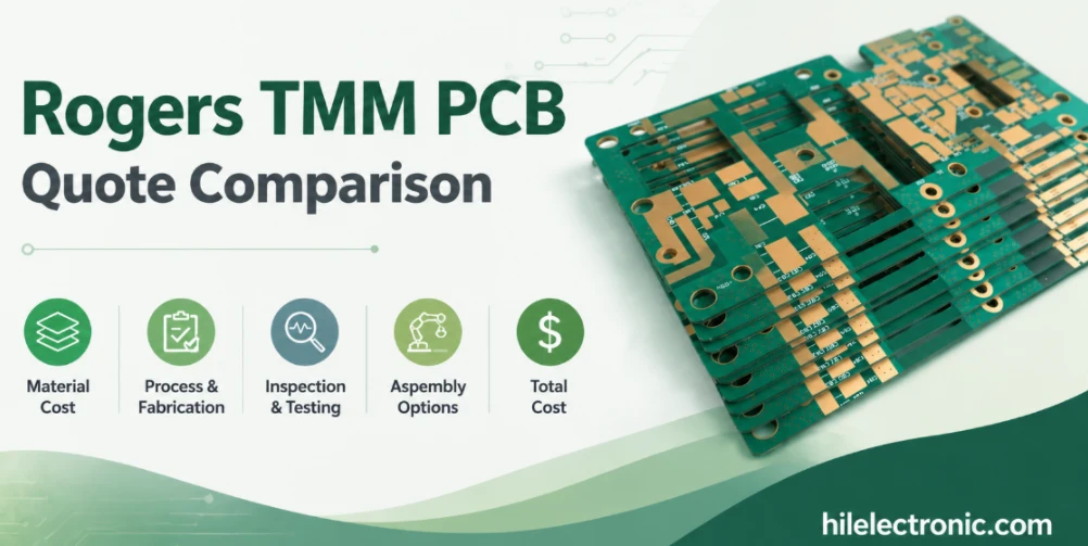
Rogers TMM PCB Quote Comparison and Cost Factors
Table of contentsCan Rogers TMM PCB Price Be Calculated...
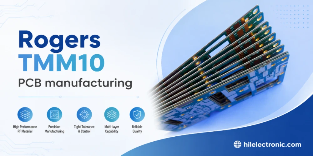
Rogers TMM10 PCB Manufacturing for RF Designs
Table of contentsHow TMM10 Shrinks RF StructuresTMM10 vs...
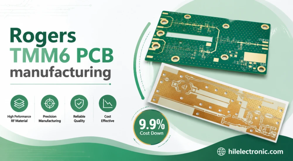
Rogers TMM6 PCB Manufacturing for Microwave Filters
Table of contentsWhy Microwave Filter Designers Use...
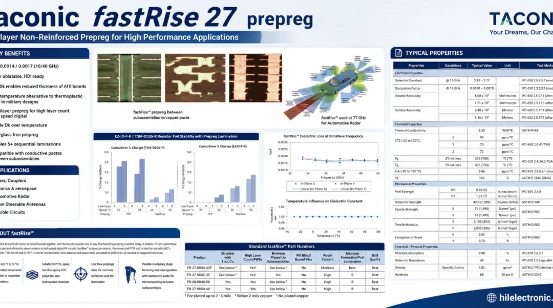
Taconic fastRise 27 Prepreg PCB Bonding and HDI Fabrication Service
Table of contentsWhat fastRise 27 Is—and What You Are...
How to get a quote for PCBs
Let‘s run DFM/DFA analysis for you and get back to you with a report. You can upload your files securely through our website. We require the following information in order to give you a quote:
-
- Gerber, ODB++, or .pcb, spec.
- BOM list if you require assembly
- Quantity
- Turn time
In addition to PCB manufacturing, we offer a comprehensive range of electronic services, including PCB design, PCBA, and turnkey solutions. Whether you need help with prototyping, design verification, component sourcing, or mass production, we provide end-to-end support to ensure your project’s success.
For PCBA services, please provide your BOM (Bill of Materials) and any specific assembly instructions. We also offer DFM/DFA analysis to optimize your designs for manufacturability and assembly, ensuring a smooth production process.