
High Aspect Ratio PCB Manufacturing for Plated Through Holes
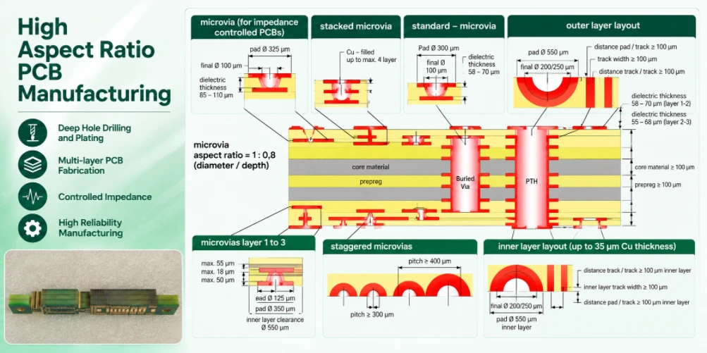
Highleap Electronics provides high aspect ratio PCB manufacturing enquiries and fabrication quotations for designs that combine thick boards with relatively small drilled holes or demanding plated-through-hole requirements. If a previous supplier has declined your design because of the board thickness, hole diameter or plating concern, send us the stackup and drill table for a construction-specific review.
For a useful high aspect ratio PCB quote, the board thickness, drill diameter, finished hole size, hole type, copper requirement and inspection plan must be defined together. Aspect-ratio capability is process-specific; a general maximum figure does not establish that every hole size, laminate and copper requirement is feasible. Highleap reviews the actual construction before confirming the appropriate manufacturing route.
Table of contents
HIGH ASPECT RATIO PCB
Thick PCB Manufacturing with Small Plated Holes
Request a High Aspect Ratio PCB Quote →This example is arithmetic only, not a statement of guaranteed manufacturing capability. Confirm the ratio against the actual drill table and plating specification.
What Is High Aspect Ratio PCB Manufacturing?
There are two aspect ratios in play on a multilayer board, and conflating them is a common source of misunderstanding with a fabricator.
| Term | Definition | Why it matters |
|---|---|---|
| Through-hole aspect ratio | Board thickness divided by finished hole diameter, so it rises with thickness and falls with hole size | Determines how well the barrel can be cleaned and plated |
| Blind and buried via aspect ratio | Depth of the via from the nearer board surface, divided by the drilled diameter, so the full board thickness is not relevant | A shallow blind via on a thick board is easy; a deep blind via is not |
| Microvia aspect ratio | Depth of the microvia from the surface it is drilled from, divided by its diameter | The tightest ratio on the board, and the one that limits build-up structures |
For a plated through-hole, the nominal aspect ratio is calculated from board thickness divided by finished hole diameter. For example, a 1.6 mm thick board with a 0.20 mm finished hole has a nominal ratio of 8:1. Microvias use a different geometry and process route: their depth-to-diameter ratio should be evaluated using the dielectric depth and via diameter, and their limits should not be compared directly with through-hole plating limits.
High Aspect Ratio PCB Drilling and Copper Plating Challenges
Three process steps degrade as the ratio rises, and they degrade for different physical reasons.
- Drilling. A long hole in a composite laminate lets the drill bit wander and lets glass fibre pull out at the exit side, which is the classic burr. Mechanical drilling of fine holes in thick material is limited by the aspect ratio that the drill geometry and the equipment can hold without deflection.
- Plating. The plating bath has to wet the full wall of the hole. In a narrow, deep hole, the solution exchange at the bottom of the barrel is slower and the copper distribution is less uniform, so the barrel copper thickness at the bottom of the via can be thinner than at the top. This is the defect that later becomes a reliability failure.
- Filling, when specified. Filling is a separate requirement from through-hole plating and introduces its own material, voiding and process constraints. The suitable fill method depends on the hole geometry and the application; do not assume every high-aspect-ratio plated through-hole should be filled.
The practical limit is not a single number, because it depends on hole diameter, board thickness, plating chemistry and whether the via has to be filled. A fabricator will quote a limit for their own process. The number that matters for your design is the one for the specific combination of hole size and thickness you need, and it should be confirmed in writing rather than assumed from a general capability list.
High Aspect Ratio PCB Via Plating Quality and Reliability
Plating uniformity inside a deep via is a reliability issue, not a cosmetic one. A plated via is a barrel of copper with a hole through it, and the electrical and thermal path runs through the barrel wall. If the wall is thin at the bottom of the barrel, the via has a lower current capacity and a higher resistance than the design assumed, and it runs hotter under load.
Three specific consequences follow, and they are worth matching to your failure history:
- Lower current capacity in the middle of the stack. A power via that appears adequate on paper may be thermally limited in the middle of the board where the copper is thinnest.
- Interconnect stress test failures that do not correlate with the defect location. An under-plated barrel is often not visible on the surface. If your boards fail an interconnect stress test at vias that look perfect, this is a first candidate.
- Poor thermal performance in filled thermal vias. A void in a filled via, or a thin plating layer, reduces the intended heat path. This shows up as a hot spot in thermal imaging rather than as a board failure.
The general principles behind plated-hole quality are covered in our PCB reliability considerations, and the specific test that catches barrel under-plating is discussed in our interconnect stress testing (IST). Improving the outcome is often a matter of the design and process choices covered in our PCB reliability improvement.
PCB Stackup Design for High Aspect Ratio Through-Holes
When a board is mechanically too thick for the via size, there are four legitimate routes. Each has a cost, and the right choice depends on which constraint is real.
| Route | How it solves the problem | What it costs |
|---|---|---|
| Increase the hole diameter | Directly lowers the aspect ratio | Density loss. On a dense design this often costs more routing area than the electrical benefit is worth |
| Reduce the board thickness | Directly lowers the aspect ratio | Mechanical and thermal. If the thickness was there for stiffness or heat spreading, it has to be replaced by something else |
| Change the via type | A blind via only has to span the layers it connects, so a thick board can carry many shallow blind vias instead of one deep through-hole | Sequential lamination cycles, and the extra process steps that come with them |
| Split the stackup | Divide the board into two laminates joined by a bonded interface, so neither half has to carry the full thickness | A bonding interface in the signal path or the thermal path, and a very tight registration requirement |
There is a fifth option that is often the cheapest: check whether the aspect ratio is actually the binding constraint, or whether it is the plating requirement behind it. Some designs are limited not by the drilling but by a requirement to fill and plate over the via, which is a stricter limit than drilling alone. The relevant processes are described in our via filling and copper plating and in our blind and buried via page.
High Aspect Ratio Through-Holes vs HDI Microvias
On a build-up board, the limiting ratio is usually the microvia rather than the through-hole. A microvia is drilled from one surface into the laminate, and it has to be plated and usually filled, in a much smaller diameter than a mechanical drill can hold.
Two factors make a microvia stack harder than its aspect ratio suggests. The first is that the microvia is blind, so the plating has to be uniform along a wall that ends in solid material rather than open at both ends, and the bottom of the barrel is where plating voids are most likely. The second is that a stack of microvias is built over a build-up structure where the copper weight per layer is high relative to the via diameter.
A practical rule is that a microvia stack of two or three levels is routine, and each additional level adds both a lamination cycle and a plating cycle with its own yield risk. If a design needs a deep stack to save routing area, it is worth reviewing the layer count against the routing requirement directly, because the two often trade against each other. The design trade-offs are set out in our HDI stackup design and the build sequence in our sequential lamination for HDI boards.
Thick PCB Manufacturing with Small Drill Holes
Thick board with heavy copper is the combination where aspect ratio problems and thermal problems compound each other, and it is where quotes tend to widen the most between suppliers.
The reason is that heavy copper has to be plated into the barrel, and plating a barrel to a heavy copper weight in a deep hole is much harder than plating it to a standard weight. The plating time is longer, the bath chemistry is pushed harder, and the risk of a plating void or a thin bottom increases. On a 3.2 mm board with 4 oz copper, the difference between a good build and a mediocre one is often the plating cycle management rather than anything the designer specified.
Three design measures reduce the difficulty:
- Use the largest via diameter the footprint allows rather than the smallest. On a power board this is usually free, because the annular ring requirement scales with the drill anyway.
- Do not fill power vias unless the thermal path requires it. Filling adds a flow step that is hard in a high ratio, and it also removes the ability to inspect the barrel visually. A resin-plugged or unfilled plated via carries more current than a copper-filled one with a void in it.
- Keep the copper weight uniform across the board rather than mixing heavy and light layers in one build, because each copper-weight change is a separate plating cycle with a separate thickness tolerance.
Backdrilling is the standard answer to a stub left by a blind via in a high-speed design, and it is discussed in our PCB backdrilling. Backdrilling itself removes material from the back of the hole, so it slightly reduces the effective barrel length and needs to be accounted for in the depth specification rather than treated as a separate afterthought.
PCB Materials for High Aspect Ratio Through-Hole Plating
On a thick board, the thermal expansion mismatch between copper and laminate becomes a bigger number, because the copper travels further in absolute terms over the board’s height. A board that survives a thermal cycle on paper can still fail at the interface between a heavy copper region and the adjacent laminate if the material system is not chosen for it.
The relevant choices are:
- Tg is the temperature at which the resin starts to soften. A board that will see soldering reflow during assembly, or a high ambient in service, needs a Tg comfortably above that exposure.
- Td is the decomposition temperature, and it is a more meaningful figure than Tg for a heavy-copper board because it indicates the margin the material retains during a press cycle.
- CTE, and specifically the CTE in the thickness direction, is the parameter that governs how much the board flexes with temperature. On a thick board, an out-of-plane CTE that is a good match to copper reduces the stress at the interface where delamination starts.
- CAF resistance matters if the board will be used in humid, high-voltage conditions, because the conductive filament grows between a via and a ground plane that are separated by the laminate.
Material selection for these requirements is covered in our high-Tg PCB materials, the broader comparison in our PCB material selection guide, and the humidity-related failure mode in our CAF resistant material page. Thermal cycling failures on thick boards are also a common reason boards are rejected at final inspection, which is described in our PCB delamination page.
Testing High Aspect Ratio PCB Plated Through-Holes
On a high aspect ratio build, the verification plan matters as much as the build. These are the methods that find the defects this process produces, and each has a specific purpose.
| Method | What it detects | What it does not detect |
|---|---|---|
| Interconnect stress test | Open circuits in the barrel, including under-plated barrels that fail at the bottom of a deep via | A via that is merely thin, but still continuous |
| Thermal cycling | Delamination and interface stress, particularly between heavy copper and laminate | Barrel plating quality |
| Microsection of a via | Actual barrel copper thickness at the top, middle and bottom of the hole; fill voids; interface quality | Anything about the rest of the panel |
| X-ray inspection | Voiding in filled vias and copper coverage in dense areas, without cutting the sample | Barrel wall thickness |
The distinction in the last column matters when you are comparing two quotations. A quotation that lists only X-ray inspection has not shown you the barrel quality. A quotation that specifies microsection on a defined sample plan has shown you how the ratio will be verified. The test methods and what each one is good for are compared in our PCB testing methods if you want the wider picture, and the drilling side of the process is in our laser drilled PCB guide.
High Aspect Ratio PCB Quote Requirements: Board Thickness and Drill Size
A quote for a high aspect ratio board is only meaningful if it is quoted against the actual geometry. Four pieces of information remove almost all of the ambiguity:
- Board thickness and layer count, with the stackup showing where the copper weight changes.
- The drill file, or at minimum the smallest and largest hole diameters and the through-hole diameter. This is the single most useful file for the fabricator, and a fabricator who asks for it before quoting is telling you they intend to quote the real process.
- Whether the vias are filled, and with what. A filled via has a lower aspect ratio limit than an unfilled one.
- The verification requirement, since microsection and stress testing add cost and time that belong in the quotation rather than being discovered later.
If a previous supplier declined the build, it is worth stating that in the RFQ along with what they objected to. If the objection was an aspect ratio limit, that is a question for the fabrication route and it may have an answer. If the objection was the price, that is also answerable. What is not answerable is a build that quietly changes the geometry to fit the process, which is why the stackup and drill file matter more than the board outline.
High Aspect Ratio PCB Manufacturer for Thick Boards and Small Holes
Highleap can review high aspect ratio PCB fabrication projects where plated-through-hole geometry, copper requirements and the selected laminate need to be evaluated together. For buyers looking for a high aspect ratio PCB manufacturer, the useful comparison is whether the supplier can support the specific board-thickness-to-hole-diameter combination and verify the finished hole-wall construction—not simply whether “high aspect ratio” appears on a capability page.
For a thick PCB with small drill holes, provide the board thickness, drill diameter, finished hole diameter, number of holes, copper weight, layer count, laminate material and applicable acceptance standard. Include microsection, interconnect stress testing or other reliability requirements if they are part of the purchase specification. These requirements can affect the process plan, test scope, lead time and quote.
When the design also includes blind or buried vias, review the full build-up through Highleap’s HDI PCB manufacturing service. For reliability-sensitive projects, the relevant interconnect stress testing and PCB reliability requirements should be stated in the RFQ. Submit the full package through the PCB quote request.
- Quote package: drill files, stackup, board thickness, drilled and finished hole dimensions, hole-wall copper requirements, quality class and required reliability tests.
High Aspect Ratio PCB Manufacturing FAQs
What aspect ratio can be built on a standard multilayer board?
It depends on hole diameter and on whether the via has to be filled, and the honest answer is that a fabricator should quote their limit against your specific combination rather than against a headline capability figure. A practical approach is to ask for the limit on your smallest through-hole and on your smallest blind via separately, since the numbers are usually different.
Does a thicker board always need thicker vias?
It raises the ratio, but the fix does not have to be a bigger via. Blind and buried vias reduce the effective depth, and separating the board into sub-stacks removes the thickness problem entirely. The question to ask is which constraint is real: routing density, current capacity, or mechanical stiffness.
Can a high aspect ratio board be filled with copper paste?
Yes, but the ratio limit is lower than for an unfilled via, because the paste has to flow the full depth of the barrel without leaving a void, and a void in a deep barrel is very difficult to detect afterwards. Where filling is not required for the thermal path, an unfilled plated via is often the more reliable choice.
Does aspect ratio affect lead time?
It can. Difficult drilling limits the number of boards a single drill cycle can produce, and heavier copper in deep barrels lengthens the plating cycle. These are real scheduling constraints on a fabricator’s capacity, not a way of quoting a slower process for the same money.
Can an existing design be restructured to lower the aspect ratio?
Very often, yes. Changing a through-hole to a blind via, increasing the smallest via diameter, or moving one layer of routing to another side of the board are all standard adjustments. It is worth asking a fabricator to review the stackup before committing to a build that is marginal, since the fix is usually small and the cost of not finding it is a scrapped panel.
HIGH ASPECT RATIO PCB · RFQ
Request a High Aspect Ratio PCB Quote
Send the Gerber, drill file, board thickness, layer count, copper weight and whether vias are filled. We check the aspect ratio against the build and quote the real route.
Drill file + stackup + fill requirement.

Recommended Posts
VIPPO PCB Fabrication for BGA and Thermal Pad Designs
Highleap Electronics provides VIPPO PCB fabrication for...

High Reliability PCB Assembly: Process Control and Traceability
Highleap Electronics manufactures high reliability PCB...
Expedited PCB Assembly: Lead Times, Readiness and Cost
Highleap Electronics offers expedited PCB assembly for...
Small-Batch High-Mix PCB Assembly for Repeat Orders
Highleap Electronics provides small-batch, high-mix PCB...
How to get a quote for PCBs
Let‘s run DFM/DFA analysis for you and get back to you with a report. You can upload your files securely through our website. We require the following information in order to give you a quote:
-
- Gerber, ODB++, or .pcb, spec.
- BOM list if you require assembly
- Quantity
- Turn time
In addition to PCB manufacturing, we offer a comprehensive range of electronic services, including PCB design, PCBA, and turnkey solutions. Whether you need help with prototyping, design verification, component sourcing, or mass production, we provide end-to-end support to ensure your project’s success.
For PCBA services, please provide your BOM (Bill of Materials) and any specific assembly instructions. We also offer DFM/DFA analysis to optimize your designs for manufacturability and assembly, ensuring a smooth production process.