
High-Frequency PCB Cost: Key Drivers and Optimization Strategies

Introduction
High-frequency PCB applications have expanded rapidly across 5G infrastructure, RF communication systems, and automotive radar technologies. These specialized circuit boards command significantly higher prices than traditional FR4 boards due to their demanding material requirements, stringent manufacturing tolerances, and precise impedance control specifications.
High-Frequency PCB cost depends on multiple interrelated factors such as material selection, manufacturing precision, and design complexity. Understanding these cost drivers enables engineers and procurement teams to make informed decisions that balance performance requirements with budget constraints.
This article examines the primary factors influencing high-frequency PCB cost and presents actionable optimization strategies to reduce expenses without compromising signal integrity or reliability in critical RF applications.
Key Cost Drivers in High-Frequency PCB Manufacturing
1. Material Selection
High-frequency materials such as PTFE, Rogers laminates, Taconic substrates, and Megtron systems cost substantially more than conventional FR4 due to their specialized dielectric properties and manufacturing complexity. The high frequency PCB material cost escalates with tighter tolerances on dielectric constant (Dk) and dissipation factor (Df) stability across temperature and frequency ranges.
Copper foil selection between rolled annealed (RA) and electrodeposited (ED) types, combined with surface roughness specifications and prepreg compatibility requirements, further impacts the PTFE vs FR4 price difference. Rogers PCB material selection decisions must balance electrical performance needs against budget realities, as premium materials can account for forty to sixty percent of total board cost.
2. Stackup and Layer Count
Multilayer high frequency PCB designs demand exceptional interlayer dielectric control and precise lamination alignment that increase manufacturing complexity proportionally with layer count. Blind and buried via structures, along with careful signal-to-ground layer pairing for impedance management, add significant fabrication steps and quality control requirements.
Six to ten layer configurations common in RF applications typically cost three to five times more than simpler two to four layer designs due to additional material usage and extended processing time. Controlled impedance stackup cost rises exponentially when tolerance windows tighten below five percent, requiring enhanced process monitoring and potential yield reduction.
3. Manufacturing Process Complexity
Fine-line geometries below seventy-five micrometers, ultra-low roughness copper treatments, and strict impedance tolerances define the high frequency PCB manufacturing process requirements that distinguish RF boards from standard products. PTFE materials require specialized drilling equipment and entry/exit materials to prevent delamination and manage the material’s tendency to smear during machining operations.
Surface finish options such as electroless nickel electroless palladium immersion gold (ENEPIG) or immersion silver add protective layers that minimize insertion loss but increase surface finish cost impact by fifteen to thirty percent compared to standard HASL treatments.
4. Yield and Process Tolerance
High-frequency materials exhibit lower dimensional stability than FR4, resulting in increased warpage during lamination cycles that reduces first-pass yield rates for complex stackups. PTFE drilling challenges including burr formation and residual copper in vias elevate rework rates and scrap levels, directly multiplying material and labor expenses.
High frequency PCB yield improvements of even five to ten percent translate into substantial cost reductions, as each rejected board carries the full burden of expensive substrate materials and extensive processing steps. PCB process tolerance control becomes increasingly critical as operating frequencies rise above ten gigahertz, where minor deviations in dielectric thickness or copper weight dramatically affect electrical performance.
5. Supply Chain and Volume
Limited supplier options for specialized RF materials create extended procurement cycles and reduced negotiating leverage that inflate RF PCB procurement costs compared to commodity materials. Small-batch custom orders typically incur price premiums of twenty-five to forty percent over high-volume production runs where material utilization and setup costs distribute across larger quantities.
Strategic inventory management and advance material procurement arrangements help mitigate supply chain delays and reduce low volume PCB cost factors by securing better pricing through volume commitments. Establishing relationships with manufacturers who maintain stock of common high-frequency materials shortens lead times and provides access to more competitive pricing structures.

High-Frequency and FR-4 Hybrid PCB
Practical Cost Optimization Strategies
1. Design for Manufacturability (DFM)
Early collaboration between design teams and fabricators enables high frequency PCB DFM practices that eliminate costly features while preserving electrical performance. Establishing realistic impedance tolerances, minimum trace widths, and via structures based on manufacturer capabilities prevents over-specification that drives up production costs unnecessarily.
Avoiding blind and buried vias where through-holes suffice, and minimizing layer count through efficient signal routing, represent straightforward design cost optimization approaches that maintain signal integrity requirements. Manufacturer design reviews before prototype fabrication identify potential yield issues and processing challenges that could escalate expenses in production phases.
2. Material Standardization
Prioritizing materials with stable supply chains and proven fabricator experience, such as Rogers 4350B, reduces procurement uncertainty and manufacturing learning curves that inflate costs. Cost-effective high frequency PCB material selection involves matching dielectric properties to actual application requirements rather than defaulting to premium substrates for marginal performance gains.
Comparing Rogers 4350B vs 4003C cost alongside electrical specifications often reveals opportunities to achieve adequate RF performance at twenty to thirty percent lower material expense. Standardizing on a smaller material palette across product lines improves purchasing leverage and enables manufacturers to optimize their processes for specific substrate characteristics.
3. Stackup Simplification
Optimizing signal and ground plane distribution to reduce unnecessary layers directly lowers material consumption and processing complexity in high frequency PCB stackup optimization efforts. Symmetric stackup architectures improve lamination consistency and reduce warpage risk, translating into higher yields and fewer rejected panels during quality inspection.
Each layer eliminated from a multilayer design typically reduces overall board cost by twelve to eighteen percent while simultaneously shortening manufacturing cycle time. Multilayer cost reduction strategies must balance electrical performance requirements against the complexity tax imposed by additional dielectric layers and interconnection structures.
4. Process Control and Yield Management
Refining drilling parameters, etching chemistry, and surface treatment sequences minimizes defects and rework cycles that compound high-frequency PCB manufacturing expenses. Implementing robust impedance control manufacturing protocols with regular coupon testing ensures boards meet specifications without extensive rework or scrapping.
PCB yield improvement initiatives that raise first-pass success rates from seventy-five to ninety percent effectively reduce per-unit costs by forty percent through better material utilization. Statistical process control and continuous monitoring of critical parameters provide early warning of drift conditions before they generate significant quantities of non-conforming boards.
5. Strategic Collaboration with Manufacturers
Sharing design parameters and target cost ranges during early project phases enables manufacturers to propose value-engineering alternatives that maintain performance while reducing expenses. Partnering with fabricators experienced in high-frequency processing and maintaining inventory of common RF materials accelerates production schedules and improves cost predictability.
At Highleap Electronics, our engineering team collaborates closely with clients to balance RF performance with cost efficiency through optimized stackup design and material sourcing. This partnership approach identifies opportunities for specification relaxation in non-critical areas while tightening controls where electrical performance demands justify additional investment.
Conclusion
High-frequency PCB cost reflects a complex interplay of material selection, design complexity, manufacturing process requirements, and yield management effectiveness. Material expenses for specialized RF substrates typically represent the largest single cost component, but manufacturing precision requirements and lower yield rates significantly amplify total project expenses. Early collaboration between design and manufacturing teams, combined with material standardization and stackup optimization, offers the most effective path to cost reduction without compromising signal integrity.
At Highleap Electronics, we leverage two decades of RF circuit board manufacturing experience to help clients navigate these cost drivers while delivering reliable high-frequency solutions. Contact our engineering team to discuss how strategic design optimization and process expertise can reduce your high-frequency PCB costs while maintaining the electrical performance your applications demand.

Recommended Posts
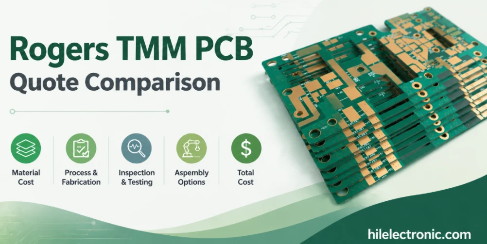
Rogers TMM PCB Quote Comparison and Cost Factors
Table of contentsCan Rogers TMM PCB Price Be Calculated...
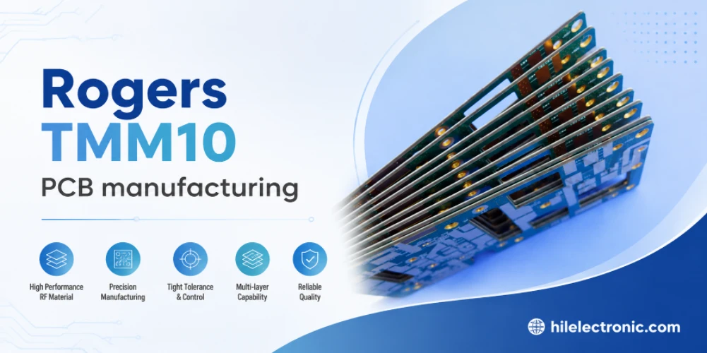
Rogers TMM10 PCB Manufacturing for RF Designs
Table of contentsHow TMM10 Shrinks RF StructuresTMM10 vs...
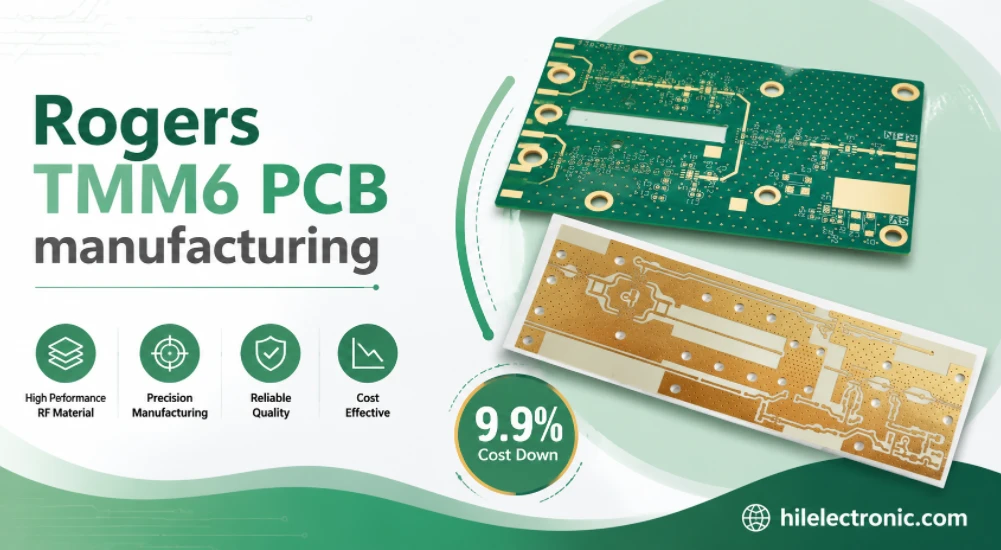
Rogers TMM6 PCB Manufacturing for Microwave Filters
Table of contentsWhy Microwave Filter Designers Use...
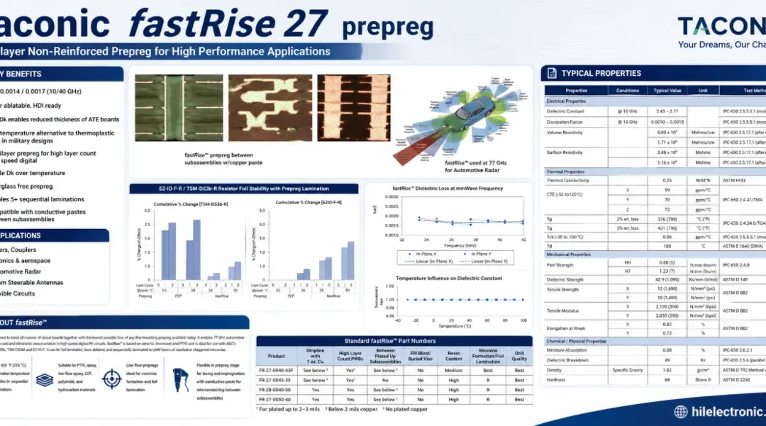
Taconic fastRise 27 Prepreg PCB Bonding and HDI Fabrication Service
Table of contentsWhat fastRise 27 Is—and What You Are...
How to get a quote for PCBs
Let‘s run DFM/DFA analysis for you and get back to you with a report. You can upload your files securely through our website. We require the following information in order to give you a quote:
-
- Gerber, ODB++, or .pcb, spec.
- BOM list if you require assembly
- Quantity
- Turn time
In addition to PCB manufacturing, we offer a comprehensive range of electronic services, including PCB design, PCBA, and turnkey solutions. Whether you need help with prototyping, design verification, component sourcing, or mass production, we provide end-to-end support to ensure your project’s success.
For PCBA services, please provide your BOM (Bill of Materials) and any specific assembly instructions. We also offer DFM/DFA analysis to optimize your designs for manufacturability and assembly, ensuring a smooth production process.