
PCB Board For Bluetooth Speaker Manufacturing

Table of Contents
Highleap Electronics manufactures the PCB board for Bluetooth speaker designs — delivering complete builds from bare PCB through assembled and tested units for global hardware developers. We handle fabrication, Bluetooth SoC sourcing, SMT assembly, and strict audio testing under one roof to ensure your product meets international market standards.
This page covers what we produce, what makes the PCB board for Bluetooth speaker applications technically different from standard electronics assembly, and what we test before worldwide delivery. For component placement rules, RF layout, and layer stackup guidance, see our Bluetooth Speaker PCB design guide.
1. PCB Boards For Bluetooth Speakers We Build
We manufacture the PCB board for Bluetooth speaker products across five main categories. Each has distinct board specifications driven by the speaker’s output power, enclosure size, and target market requirements.
| Board Category | Typical Specification | Application |
|---|---|---|
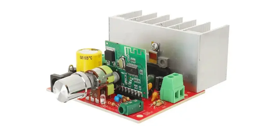
| Portable speaker mainboard | 2-layer FR4, 1.6 mm, ENIG, 5W Class D, Li-ion charging | Outdoor portable speakers, desktop mini speakers |
| Compact enclosure board | 2-layer FR4, 0.8–1.0 mm, ENIG, board outline matched to enclosure | Miniature speakers, wearable audio products |
| High-output speaker board | 4-layer FR4, 1.6 mm, ENIG, 10–20W Class D, 2 oz copper on power layer | Party speakers, commercial audio, stage monitors |
| Smart speaker mainboard | 4-layer FR4, 1.6 mm, ENIG, Bluetooth 5.x + Wi-Fi coexistence management | Voice assistant devices, smart home audio |
| Automotive in-vehicle speaker | 4-layer FR4, −40°C to +85°C rated, AEC-Q100 qualified ICs | Connected vehicle audio, V2X, telematics |
Designs outside these categories are not a problem. Send us your Gerber files and BOM and we will confirm whether we can build it. Most first-time designs go from DFM review to shipped prototype within two weeks, supporting agile development teams globally.
For multi-driver and crossover configurations beyond a single Bluetooth unit, our speaker PCB manufacturing page covers amplifier boards, DSP boards, and complete audio system builds.
2. What Makes These Boards Different to Manufacture
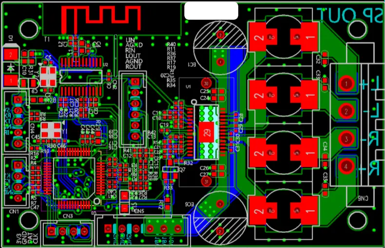
The PCB board for a Bluetooth speaker is not a standard consumer electronics circuit. It carries three electrically incompatible environments on a single board — and the way those environments interact during manufacturing and assembly creates failure modes that do not exist on ordinary digital boards.
The RF environment and the analog audio environment cross-contaminate. The Bluetooth SoC switches at 2.4 GHz. The Class D amplifier switches at 300–500 kHz. Placed too close together, the amplifier’s switching harmonics degrade the SoC’s receive sensitivity — which shows up as reduced Bluetooth range, not as an assembly defect. A DFM review catches this before fabrication. An assembler without DFM capability ships boards that pass functional test but fail in the field beyond 5 meters, risking your brand’s reputation in local markets.
Bluetooth SoC components are highly lead-time-sensitive. Qualcomm (QCC3040, CSR8635), Realtek (RTL8763E), and Nordic Semiconductor (nRF52832) all have lead times that shift rapidly depending on global demand cycles. A supplier who sources your SoC tells you the confirmed lead time before you place the order. A supplier who only assembles boards hands the supply chain risk back to you.
The reflow profile for a Bluetooth speaker board cannot be generic. The Bluetooth SoC’s exposed thermal pad and the Class D amplifier’s PowerPAD have different thermal masses and different minimum solder temperatures. A single reflow profile optimised for passive components will underheat the SoC’s fine-pitch pads — producing boards where Bluetooth pairs but one audio channel is absent or intermittent.
These factors are why producing a high-quality PCB board for Bluetooth speaker applications benefits from a single manufacturing team that controls fabrication, global component sourcing, and assembly together.
3. Assembly Requirements Unique to Bluetooth Audio
The assembly challenges on a PCB board for Bluetooth speakers are specific to the combination of Bluetooth SoC, Class D amplifier, and battery management circuit sharing one board.
Bluetooth SoC exposed pad coverage: 70–80% minimum. The QFN-packaged Bluetooth SoC has a large exposed thermal pad on its underside. Paste coverage below 70% creates voids that increase thermal resistance and raise operating temperature — the SoC hits its thermal throttle threshold during sustained audio playback at high volume. We confirm coverage with 3D SPI before every board enters the oven.
RF matching network bridges: the failure functional test misses. A solder bridge between two adjacent pads in the RF matching network shifts the antenna impedance away from 50Ω. The board passes power-on test, but Bluetooth range drops from 10 meters to 3–4 meters. Our AOI program specifically checks the RF matching network pads for bridges, ensuring reliable connectivity for end-users worldwide.
Class D output filter inductor orientation. The two output filter inductors on a Class D amplifier board must be mounted perpendicular to each other. Parallel placement couples switching energy back into the audio signal path, raising the output noise floor. It must be verified by AOI rotation check.
Reflow profile: 245°C minimum at the SoC body for 30–60 seconds. We profile with a thermocouple directly on the SoC package. Underheating produces the most common audio assembly failure: correct Bluetooth pairing but audio output on one channel only.
For the process controls that govern Class D output stages, our audio amplifier assembly resource covers these in full.
4. Audio and RF Testing for Global Compliance
Generic PCB assembly testing is insufficient for a PCB board for Bluetooth speaker devices. These boards require product-specific tests that confirm the RF section, audio section, and power management section all perform to specification, ensuring compliance with FCC, CE, and other international standards.
| Test | Pass Criteria | When Applied |
|---|---|---|
| Bluetooth pairing and range check | Pairs in <5 seconds; maintains connection at minimum 8 m in open space | Every unit |
| Dual-channel audio output | Audio present on both L and R channels; no single-channel failure | Every unit |
| THD — total harmonic distortion | <1% at rated output power (e.g. 5W or 10W as specified) | First articles; sampling at production volume |
| Frequency response | ±3 dB from 80 Hz to 15 kHz at 1W reference output | First articles; sampling at production volume |
| SNR — signal-to-noise ratio | >80 dB at rated output; idle hiss below −80 dBFS | First articles; any unit flagged by audio test |
| Battery charge termination | Charge terminates at 4.2V ±0.05V; overvoltage protection activates correctly | Every unit with charging circuit |
| RF coexistence (FCC/CE focus) | No Bluetooth dropouts over 30 minutes with a 2.4 GHz Wi-Fi router active at 1 m | First articles; mandatory for smart home speaker designs |
The range check and dual-channel audio test run on every unit. The THD, frequency response, and SNR tests run on first articles and are available on request for production sampling. For smart home speakers that combine Bluetooth with Wi-Fi, the coexistence test is mandatory and we extend it to include 5 GHz Wi-Fi active simultaneously.
5. Global Lead Times, Pricing, and How to Order
We partner with international logistics providers (DHL, FedEx, UPS) to ensure rapid global shipping to North America, Europe, and beyond.
| Service | Lead Time | Notes |
|---|---|---|
| Bare PCB — 2-layer FR4 | 3–5 business days | Rush 24–48 hr available for qualifying designs |
| Bare PCB — 4-layer, controlled impedance | 5–7 business days | Includes TDR impedance verification on antenna trace |
| Turnkey assembly — Bluetooth SoC in stock | 7–14 business days | PCB fab and component sourcing run in parallel |
| Turnkey assembly — Bluetooth SoC on order | SoC lead time + 5 days assembly | We confirm SoC availability before you order |
Minimum order quantity: No minimum for bare PCB fabrication. Assembly starts at 5 units for prototype builds. Production pricing begins at 50 units.
What drives the price of a PCB board for Bluetooth speakers: Layer count; surface finish (ENIG is required for QFN SoC packages); Bluetooth SoC unit cost at your quantity; and testing level.
What to send us: Gerber files, BOM with manufacturer part numbers, pick-and-place centroid file, and your target quantity and delivery region. We return a detailed quote within 24 hours for standard designs. For your broader consumer electronics PCB requirements, our capabilities cover the full range of IoT and smart home products.
For detailed specifications on bare board production standards, see our PCB fabrication page. For assembly capabilities across all product categories, see our PCB assembly services.
Request a PCB Board For Bluetooth Speaker Quote
Frequently Asked Questions
Can you manufacture a PCB board for Bluetooth speaker from my Gerber files?
Yes. Send your Gerber files, BOM, pick-and-place centroid file, and stackup specification. We run a DFM review within 24–48 hours covering antenna keepout zone compliance, SoC decoupling placement, and RF matching network pad geometry — issues specific to Bluetooth boards that generic DFM tools do not check.
Do you source the Bluetooth SoC for my build globally?
Yes, as part of our turnkey service. We source Qualcomm, Realtek, Nordic Semiconductor, and other Bluetooth SoC variants from authorized global distributors. We check availability and confirm your lead time before you place the order.
What is the minimum order quantity for PCB board for Bluetooth speaker assembly?
No minimum for bare PCB fabrication. Assembly orders start at 5 units for prototype builds. If you need a single board for development and testing, contact us — we handle one-off builds at a prototype rate with worldwide shipping. Production pricing begins at 50 units.
How do you confirm a board works before it ships?
Every assembled board goes through a power-on functional test: Bluetooth pairing confirmation, audio output on both channels, and battery charge initiation. First-article orders also include Bluetooth range verification at 8 meters. Any board that fails a test does not ship until the failure is diagnosed, corrected, and retested.
Can you handle both the prototype and the production run for the same design?
Yes. The same DFM review, the same Bluetooth SoC source, the same reflow profile verified against your specific board, and the same audio test procedure carry forward from first article to volume production. When your prototype passes testing, the production qualification is already documented.

Recommended Posts

Custom Rogers RO4835 PCB Fabrication & Assembly Services
Figure 1. Rogers RO4835 PCBRogers RO4835 PCB is a...

Nelco N4000-13 PCB Material and Manufacturing Guide | Highleap Electronics
Figure 1. Nelco N4000-13 PCBNelco N4000-13 PCB is a...

Rogers RT/duroid 6002 PCB Manufacturer — Specifications, Stackup, Quote
Figure 1. Rogers RT/duroid 6002Rogers RT/duroid 6002 is...

Miniaturize Antennas with Rogers TMM Laminates
Figure 1. Rogers TMM Executive Summary: Rogers TMM...
How to get a quote for PCBs
Let us run DFM/DFA analysis for you and get back to you with a report.
You can upload your files securely through our website.
We require the following information in order to give you a quote:
-
- Gerber, ODB++, or .pcb, spec.
- BOM list if you require assembly
- Quantity
- Turn time