
Analysis the PCBA Faults and Defect Resolution Measures

Table of Contents
- PCBA Reliability in Modern Electronics
- Failure Mechanisms: Root Causes and System-Level Impact
- Design-Level Risk Analysis and Preventive Engineering
- Manufacturing Defect Mechanisms and Process Controls
- Field Stress, Handling Damage and Lifetime Degradation
- Environmental Degradation and Material Aging
- Advanced PCB Failure Analysis Methodologies
- Building a Closed-Loop Reliability Strategy
Printed Circuit Board Assembly (PCBA) is the structural and functional backbone of modern electronic systems — from consumer devices and industrial automation to medical instrumentation and aerospace platforms. As integration density increases and component geometries shrink, reliability margins narrow dramatically. A single micro-crack, void, contamination site, or impedance discontinuity can cascade into catastrophic field failure.
Therefore, PCBA reliability is no longer a downstream inspection problem — it is a multidisciplinary engineering discipline that spans design architecture, materials science, process control, environmental physics, and lifecycle management. This article presents a systematic technical framework for understanding failure mechanisms, root cause analysis, and preventive engineering strategies across the entire PCBA lifecycle.
1) PCBA Reliability in Modern Electronics
Electronics failure rarely occurs instantaneously. Most failures originate as microscopic structural or chemical anomalies introduced during design or fabrication, then evolve under thermal, mechanical, electrical, or environmental stress.
1.1 Reliability Is a System Property
PCBA reliability is influenced by:
- Electrical design margin
- Material compatibility and CTE matching
- Solder metallurgy stability
- Moisture sensitivity level (MSL)
- Assembly process capability (Cpk)
- Environmental stress exposure
Effective reliability engineering integrates these domains rather than treating failures as isolated defects. For manufacturability-risk prevention, integrate DFM early (see free DFM review checklist).
2) Failure Mechanisms: Root Causes and System-Level Impact
2.1 Primary Failure Categories
| Category | Typical Root Causes | Failure Manifestation |
|---|---|---|
| Design Deficiencies | Inadequate clearance, poor grounding, thermal miscalculation | EMI failure, overheating, intermittent operation |
| Manufacturing Defects | Solder bridges, voids, plating defects | Short circuit, open circuit, yield loss |
| Handling / Usage Damage | ESD, vibration, thermal cycling | Latent component degradation |
| Environmental Exposure | Humidity, oxidation, contamination | Electrochemical migration, corrosion |
2.2 Common Failure Effects
- Signal attenuation or distortion
- Intermittent contact behavior
- Thermal runaway
- Conductive anodic filament (CAF)
- Dielectric breakdown
- Complete functional collapse
3) Design-Level Risk Analysis and Preventive Engineering
3.1 Insufficient Clearance and Creepage
Clearance violations are a leading cause of arc discharge, solder bridging, and conductive contamination. Spacing must consider:
- Operating voltage
- Environmental pollution degree
- Manufacturing tolerance stack-up
- Conformal coating thickness
Modern DRC should incorporate IPC-2221 and IPC-9592 guidelines rather than generic CAD defaults.
3.2 Electromagnetic Compatibility (EMC) Deficiencies
Poor return path control, split reference planes, or insufficient decoupling induce radiated and conducted emissions.
Preventive strategies include:
- Continuous ground plane under high-speed traces
- Controlled impedance routing
- Minimized loop area
- Common-mode choke integration
- Ferrite suppression on I/O interfaces
3.3 Thermal Mismanagement
High-power density components require junction-to-ambient thermal modeling. Neglecting copper weight, via stitching density, or airflow direction accelerates solder fatigue and component drift.

4) Manufacturing Defect Mechanisms and Process Controls
4.1 Solder Bridging and Wetting Imbalance
Root causes:
- Stencil aperture misdesign
- Excess solder paste deposition
- Reflow temperature overshoot
- Component misalignment
Preventive actions (SMT execution details here: SMT PCB assembly process):
- SPI (Solder Paste Inspection)
- Reflow profile optimization
- Nitrogen atmosphere control
- AOI + X-ray validation
4.2 Plating Voids in PTH
Void formation results from inadequate desmear, drilling smear residue, or trapped air during electroplating.
Advanced control methods include:
- Pulse plating current modulation
- Plasma desmear uniformity verification
- X-ray cross-sectional validation
- Statistical plating thickness monitoring
4.3 Ionic and Organic Contamination
Flux residue or Na+/Cl− ionic contamination can reduce Surface Insulation Resistance (SIR) and trigger dendritic growth.
Mitigation includes:
- DI water cleaning validation
- ROSE testing
- Ion chromatography analysis
- Cleanroom air filtration
5) Field Stress, Handling Damage and Lifetime Degradation
5.1 Electrostatic Discharge (ESD)
ESD damage can be catastrophic or latent. Even sub-visible oxide breakdown shifts transistor parameters.
- Grounded wrist straps
- Conductive packaging
- TVS diodes
- ESD floor systems
5.2 Thermal Cycling Fatigue
CTE mismatch between copper (17 ppm/°C), FR4 (~14–18 ppm/°C), and solder (~22 ppm/°C) generates cyclic stress.
- Underfill for BGA packages
- Thicker copper layers
- Low modulus encapsulants
- Interposer layers
5.3 Mechanical Shock and Vibration
High-cycle vibration induces micro-cracks at solder joints and via barrels.
- Conformal coating
- Mechanical reinforcement for heavy components
- Potting compounds
- Shock isolation mounts
6) Environmental Degradation and Material Aging
6.1 Oxidation and Surface Finish Instability
Copper oxidation increases contact resistance and reduces solderability.
- ENIG (Ni/Au barrier)
- Immersion silver
- OSP protection
- Hermetic packaging
6.2 Moisture-Induced Failure
Moisture ingress leads to:
- CAF formation
- Dielectric breakdown
- Polymer swelling
- Popcorn cracking during reflow
Moisture barrier bags, baking protocols, and hydrophobic coatings are essential mitigation measures. For harsh environments, learn about conformal coating.
7) Advanced PCB Failure Analysis Methodologies
7.1 Non-Destructive Techniques
- Visual inspection (optical microscopy)
- X-ray fluoroscopy (BGA, void detection) — see X-ray inspection guide
- Scanning Acoustic Microscopy (SAM)
- Infrared thermography
7.2 Destructive & Analytical Techniques
- Cross-section micro-slicing
- Scanning Electron Microscopy (SEM)
- Energy Dispersive Spectroscopy (EDS)
- X-ray Photoelectron Spectroscopy (XPS)
- Differential Scanning Calorimetry (DSC)
- Thermomechanical Analysis (TMA)
These methods enable metallurgical characterization, intermetallic thickness measurement, contamination identification, and Tg validation. For inline defect screening, also reference AOI inspection.
8) Building a Closed-Loop Reliability Strategy
True PCBA reliability requires:
- Design for Manufacturability (DFM)
- Design for Reliability (DFR)
- Statistical Process Control (SPC)
- Failure Mode and Effects Analysis (FMEA)
- Root Cause Corrective Action (RCCA)
- Continuous Improvement Feedback Loop
No manufacturing process is flawless. However, systematic understanding of defect physics enables elimination of root causes rather than temporary containment. If you need an end-to-end build + inspection workflow, consider turnkey PCB assembly.
Contact us today for a comprehensive PCBA failure analysis service.
Sabrina has over 18 years of experience in the PCB industry, with a strong background in CAM engineering and PCB file review. She supports PCB projects from prototype to volume production, focusing on manufacturability and process reliability. Her work helps engineering teams reduce production risk and achieve stable, high-quality PCB manufacturing results.

Recommended Posts

Clean Flux vs No-Clean Flux: Residue, Cleaning, and PCB Reliability
Figure 1. clean flux vs no-clean flux image for Highleap...
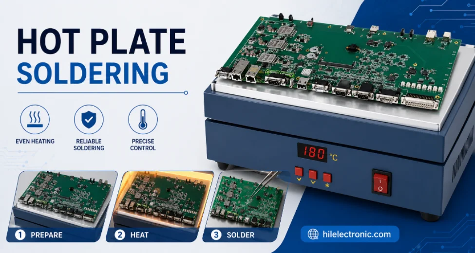
Hot Plate Soldering: Process, Limits, and Reflow Comparison
Figure 1. hot plate soldering image for Highleap...
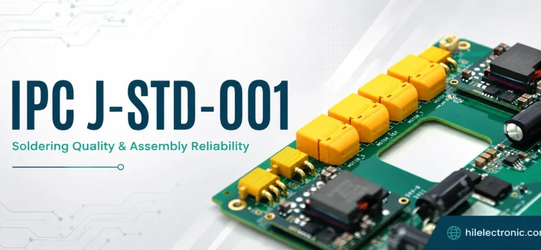
IPC J-STD-001: Classes, Requirements, and RFQ Specification
Figure 1. IPC J-STD-001 image for Highleap Electronics PCB...
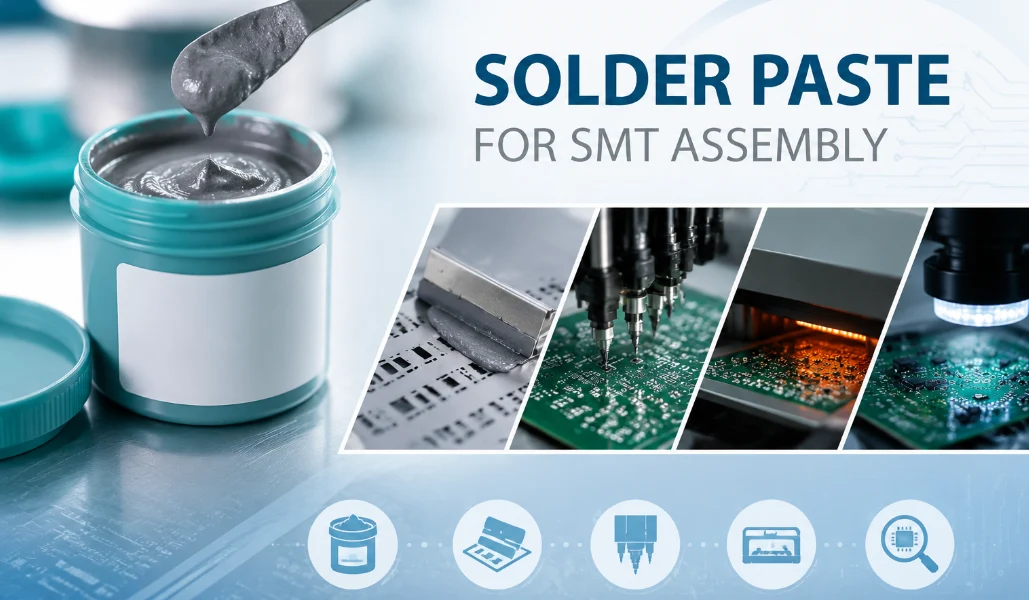
Solder Paste for SMT Assembly: Types, Storage, and Printing Defects
Figure 1. Solder paste selection affects SMT print...