
Pick and Place File Requirements for PCB Assembly

Table of Contents
- What Pick and Place Files Contain
- File Format Specifications
- Coordinate Systems and Origins
- Rotation Conventions
- Common Errors and Solutions
- Generating Quality Placement Files
At Highleap Electronics, we manufacture PCBs and run SMT assembly builds every day. A pick and place file is only “correct” when it matches the actual production board data (Gerber outline, drill, BOM revision, panelization). This guide explains practical pick and place file requirements so your placement program can be created quickly and accurately.
1. What Pick and Place Files Contain
Pick and place files (also called centroid or XY placement files) provide machine-readable component location data used to program SMT pick-and-place equipment. In production, the placement file is cross-checked against Gerber and BOM to ensure the coordinates and orientations match the real PCB being built.
1.1 Required Data Fields
- Reference Designator: Component identifier (R1, C5, U3) that must match the BOM
- X Coordinate: Horizontal position from the defined origin
- Y Coordinate: Vertical position from the defined origin
- Rotation: Component orientation in degrees
- Side: Top or Bottom of board
1.2 Optional Helpful Fields (Recommended)
- Component Value / Description: 10k, 100nF, MCU model, etc.
- Footprint / Package: 0402, 0603, SOT-23, QFN-32, LQFP-48, etc.
- Manufacturer Part Number (MPN): Speeds up kitting and reduces sourcing questions
If you’re preparing a full manufacturing handoff (Gerbers, drill, BOM, placement, drawings), this checklist can help ensure nothing is missing:
PCB assembly file requirements.
2. File Format Specifications
2.1 Accepted Formats
CSV (Comma-Separated Values): The most common and universally accepted format (.csv).
TXT (Tab-Delimited): A widely accepted alternative (.txt), especially from some CAD exports.
2.2 File Structure Best Practices
- Include a header row (column names) and keep it consistent.
- Keep X/Y/Rotation as numeric-only fields (no symbols, no mixed text).
- Use consistent precision (for example, 3–4 decimal places).
- Avoid comments or extra rows inside the data region (machines and scripts may misread them).
2.3 File Structure Example
R1,10.500,25.300,0,Top,10K,0402
C1,15.000,30.100,90,Top,100nF,0603
U1,50.000,40.000,0,Top,STM32F103,LQFP48
Some CAD tools label the same export as “centroid.” If you need a field-by-field explanation of centroid outputs and naming differences, you can reference:
Centroid file specifications.
3. Coordinate Systems and Origins
Coordinate errors are the most common reason a placement file looks “reasonable” but fails in production. The key is clarity: the factory must know exactly what your X/Y numbers are measured from and in what units.
3.1 Origin Point
- Lower-left corner: Most common and recommended for single-PCB coordinates
- Center of board: Sometimes used—must be clearly specified and consistently applied
Always state your origin clearly. In real SMT programming, an origin mismatch typically produces a “uniform offset” where every component shifts by the same distance relative to the board outline.
3.2 Units Specification
- Millimeters (mm): International standard and preferred
- Mils: US legacy unit (1 mil = 0.0254 mm)
Always specify units. A unit mismatch causes scaling errors that can place parts off-board or inside keep-out areas.
3.3 Panel vs. Single PCB Coordinates (Important for Assembly)
If your PCB will be assembled in a panel, confirm whether your file is:
- Single-PCB coordinates: The factory applies panel offsets during machine programming (common approach)
- Panel coordinates: Your file already includes offsets/tooling rails (valid, but must be labeled clearly)
Panelization decisions (tooling rails, fiducials, breakaway style, keep-outs) directly affect assembly yield and programming time. If you’re finalizing the design for manufacturing, this guide is a practical reference: Assembly design rules.
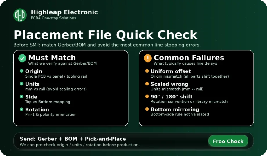
4. Rotation Conventions
Rotation is the second most common cause of assembly problems, especially for polarized parts and bottom-side placement. The goal is not to follow a “universal” theory—it’s to ensure the rotation exported by your CAD matches the intended orientation on the real PCB.
4.1 Standard Convention
- 0°: Component in zero-rotation position
- 90°: Rotated 90° counterclockwise
- 180°: Rotated 180°
- 270°: Rotated 90° clockwise
4.2 Zero Rotation Reference (How factories verify it)
ICs: Pin 1 orientation is the key reference. A correct pick-and-place file must match the assembly view/silkscreen Pin 1 marking.
Polarized parts (diodes/LEDs/electrolytics): Must match polarity marks (K stripe, + sign, notch/stripe).
Chip components: Typically aligned with their long axis along the X-axis (varies by library, so consistency matters).
Bottom-side note: Bottom placement can involve mirroring rules depending on CAD export behavior. A fast factory-style check is to validate one bottom-side polarized component in your 3D/assembly view—if it’s correct, the bottom-side convention is usually correct for the whole board.
5. Common Errors and Solutions
5.1 Coordinate Errors
Origin mismatch: All components are uniformly offset—verify the origin matches the Gerber board outline and that you’re not mixing single-board vs panel origins.
Unit mismatch: Wrong scale—explicitly specify mm or mil and regenerate the file if needed.
5.2 Rotation Errors
All rotations wrong (consistent offset): Different zero-rotation convention—verify using one IC (Pin 1) and one polarized component, then document the convention used.
Some rotations wrong (isolated parts): Inconsistent footprints—verify those specific footprints against datasheets and your assembly view.
5.3 Missing Data
Components missing: Include all placed components required for assembly (and fiducials if your process requires them).
Mismatched designators: Generate Gerbers/BOM/placement from the same design revision to avoid RefDes conflicts.
6. Generating Quality Placement Files
6.1 CAD Export Checklist
- ☐ Origin set and documented (lower-left recommended for single PCB)
- ☐ Units clearly defined (mm recommended)
- ☐ Top/Bottom side correctly exported
- ☐ All components included (and fiducials if required)
- ☐ Header row included and columns are consistent
6.2 Verification Checklist (Before sending to assembly)
- ☐ Coordinates fall within board dimensions (sanity check against outline)
- ☐ Verify one top-side IC orientation (Pin 1)
- ☐ Verify one bottom-side polarized component orientation (mirroring rule)
- ☐ Top/Bottom correctly assigned
- ☐ Reference designators match BOM quantity and naming
If you want an extra safety step for first articles, new footprints, or tight mechanical constraints, a quick DFM review often catches origin/rotation/polarity risks before production starts:
Free DFM review.
Contact Highleap Electronics for help generating or verifying pick and place files for PCB assembly—especially if you’re unsure about origin, panel coordinates, or bottom-side rotation conventions.

Charles has over 10 years of experience in PCB CAM engineering and electronics manufacturing, specializing in PCB file verification, DFM analysis, and production preparation for multilayer, HDI, RF, and high-speed boards. Proficient in Genesis, InCAM, and CAM350, he ensures accurate data, stable processes, and high manufacturing yield.
At Highleap Electronics, he focuses on process optimization and manufacturability evaluation to help customers reduce risks, shorten lead times, and achieve reliable production results.

Recommended Posts

Wireless Mechanical Keyboard PCB Manufacturing
Table of contentsWireless Keyboard PCB Procurement...

Split Keyboard PCB Manufacturing & Assembly
Table of contentsSplit Keyboard PCBA Procurement...
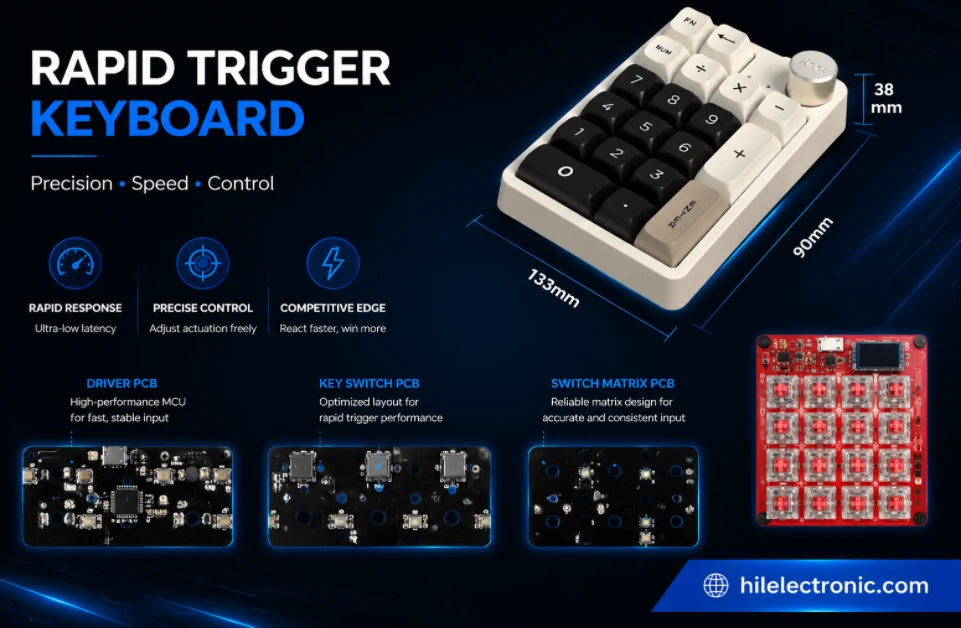
Rapid Trigger Keyboard PCB Manufacturing & PCBA
Table of contentsRapid Trigger PCBA Buying and Performance...
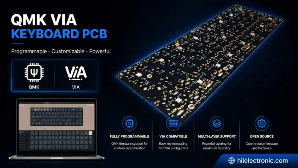
QMK/VIA Keyboard PCB Manufacturing & Assembly
Table of contentsQMK/VIA Keyboard PCB Buying...
How to get a quote for PCBs
Let us run DFM/DFA analysis for you and get back to you with a report.
You can upload your files securely through our website.
We require the following information in order to give you a quote:
-
- Gerber, ODB++, or .pcb, spec.
- BOM list if you require assembly
- Quantity
- Turn time
In addition to PCB manufacturing, we offer a comprehensive range of electronic services, including PCB design, PCBA (Printed Circuit Board Assembly), and turnkey solutions. Whether you need help with prototyping, design verification, component sourcing, or mass production, we provide end-to-end support to ensure your project’s success. For PCBA services, please provide your BOM (Bill of Materials) and any specific assembly instructions. We also offer DFM/DFA analysis to optimize your designs for manufacturability and assembly, ensuring a smooth production process.