
What is a Mixed-Signal PCB? Complete Overview and Design Fundamentals

What is a Mixed-Signal PCB?
A mixed-signal PCB integrates both analog and digital circuits on a single printed circuit board, enabling signal acquisition, processing, and communication within one unified platform. This integration has become critical as industries advance toward IoT, 5G communications, and medical devices. Mixed-signal PCB architecture allows engineers to optimize system performance while reducing footprint and interconnection delays, making it essential for modern electronics where continuous analog signals and discrete digital logic must coexist.
Understanding Mixed-Signal PCB Systems
Analog and Digital Signal Characteristics
Analog signals are continuous waveforms representing physical quantities with infinite resolution, making them highly sensitive to noise and interference. Digital signals operate through discrete voltage levels with rapid switching transitions that generate electromagnetic interference affecting nearby analog components. The fundamental challenge in mixed-signal PCB design stems from these contrasting behaviors operating simultaneously on the same substrate.
Signal Conversion Interfaces
Analog-to-digital converters (ADC) and digital-to-analog converters (DAC) serve as critical bridges between analog and digital domains in mixed-signal PCB applications. These conversion interfaces determine overall system performance by translating continuous analog measurements into digital data for processing, then reconstructing analog outputs when required. The essence of effective mixed-signal PCB design lies in balancing measurement precision with processing speed while maintaining signal integrity across both domains.
Mixed-Signal PCB Structure and Layer Configuration
Stackup Architecture
Mixed-signal PCB designs typically employ four or more layers to provide adequate separation and shielding. A standard stackup includes dedicated signal layers alternating with ground and power planes, creating controlled impedance paths and minimizing crosstalk. This multilayer approach enables physical partitioning of analog and digital regions while maintaining a common ground reference plane for consistent voltage references.
Regional Partitioning Strategy
Physical separation of analog and digital sections on a mixed-signal PCB reduces electromagnetic coupling and prevents high-frequency digital noise from contaminating sensitive analog measurements. Ground planes must be carefully planned to avoid ground loops while ensuring proper return paths for each circuit domain. High-frequency sections in mixed-signal PCB designs often require low-loss dielectric materials to minimize signal attenuation and maintain phase consistency, particularly in RF applications.
Key Design Considerations for Mixed-Signal PCB
Signal Integrity Management
Signal integrity represents the primary challenge in mixed-signal PCB design, as high-speed digital switching induces noise into adjacent analog circuits through capacitive and inductive coupling. Critical analog signal paths require careful impedance control and isolation from digital clock lines and data buses. Proper trace routing, spacing, and shielding techniques preserve signal quality across both domains on the mixed-signal PCB.
Power Distribution and Decoupling
Power supply noise isolation through effective filtering and power distribution network (PDN) design prevents digital switching currents from corrupting analog supply rails. The mixed-signal PCB power architecture must deliver clean voltage references to precision analog circuits while handling dynamic current demands of digital logic. Implementation strategies include:
- Separate voltage regulators – Independent power supplies for analog and digital sections eliminate shared impedance coupling.
- Strategic decoupling capacitors – Placement near power pins minimizes supply bounce and high-frequency noise propagation.
- Isolated ground returns – Dedicated return paths prevent digital switching currents from flowing through analog ground planes.
Clock and Reference Management
Clock signal management in mixed-signal PCB systems directly impacts both digital timing accuracy and analog measurement precision. Dedicated clock routing with proper termination and isolation from sensitive analog paths prevents timing degradation and jitter. Reference voltage distribution requires low-impedance paths with minimal interference to ensure accurate ADC and DAC operation throughout the mixed-signal PCB.

Material and Manufacturing Factors for Mixed-Signal PCB
Substrate Material Selection
Mixed-signal PCB fabrication utilizes various materials depending on performance requirements. FR4 serves cost-effective designs, while high-performance applications require Rogers, Megtron, or hybrid stackups. The dielectric constant (Dk) and dissipation factor (Df) of substrate materials significantly affect high-frequency signal attenuation and phase consistency. Material selection must balance electrical performance with thermal stability and manufacturing feasibility.
Manufacturing Precision Requirements
Copper thickness uniformity and interlayer dielectric thickness control are critical manufacturing parameters impacting mixed-signal PCB performance. Tight tolerances on trace geometry and layer registration ensure consistent impedance and minimize signal distortion. Collaboration with experienced manufacturers during design phases helps optimize stackup structure and material selection for manufacturability while meeting electrical specifications.
Typical Applications of Mixed-Signal PCBs
Communication and Wireless Systems
Mixed-signal PCB technology forms the foundation of wireless communication modules where RF transceivers interface with digital signal processing units. These applications demand precise integration of analog front-ends for signal conditioning with high-speed digital processors. The mixed-signal PCB architecture enables compact designs for cellular base stations, Wi-Fi routers, and satellite communication equipment.
Medical and Industrial Electronics
Medical monitoring devices rely on mixed-signal PCB designs to capture analog biosignals through sensors and convert them to digital data for display and analysis. Industrial control systems utilize mixed-signal PCBs to interface analog sensor inputs with digital controllers and communication networks. Automotive ADAS (Advanced Driver Assistance Systems) integrate analog sensor signals from cameras and radar with digital processing units for real-time computation.
Consumer and IoT Devices
Smart wearable devices and IoT nodes employ mixed-signal PCB technology combining sensor interfaces, wireless connectivity, and microcontroller functions in compact form factors. These consumer applications benefit from space savings and performance optimization that mixed-signal integration provides. The growing demand for intelligent connected devices continues to drive innovation in mixed-signal PCB design techniques and manufacturing capabilities.
Advantages and Challenges of Mixed-Signal PCB Design
Integration Benefits
Mixed-signal PCB architecture delivers multiple advantages for modern electronic systems:
- High integration density – Combining analog and digital functions on a single board optimizes system performance and reduces assembly complexity.
- Reduced interconnection latency – Minimized distances between circuit sections improve response times and signal quality.
- Lower manufacturing costs – Consolidated designs reduce component count, assembly steps, and overall space requirements compared to separate board implementations.
Design and Manufacturing Challenges
The primary challenge in mixed-signal PCB development involves controlling interference between analog and digital circuits sharing the same substrate and ground planes. Design complexity requires expertise spanning circuit design, electromagnetic compatibility, and manufacturing processes. Tight manufacturing tolerances and material selection add cost considerations that must balance against performance requirements for each specific mixed-signal PCB application.
Conclusion
Mixed-signal PCBs enable the sophisticated electronic systems powering modern technology by bridging precision analog measurement with high-speed digital processing. Success requires considering material properties, layer stackup, and manufacturing parameters from the earliest design stages to ensure performance stability and reliability. The careful balance of analog precision and digital speed, combined with proper isolation techniques, determines the effectiveness of any mixed-signal implementation.
Highleap Electronics Mixed-Signal PCB Capabilities
Highleap Electronics delivers comprehensive mixed-signal PCB solutions through:
- Advanced manufacturing capabilities – Precision fabrication with tight tolerance control for complex multilayer stackups and high-frequency materials.
- Technical design support – Collaborative engineering assistance for stackup optimization, material selection, and EMC compliance.
- Quality assurance – Rigorous testing and inspection processes ensuring reliable performance across analog and digital domains.
- Full assembly services – Component procurement, SMT placement, and functional testing for complete turnkey solutions.
Partner with Highleap Electronics for your next mixed-signal PCB project. Our experienced team combines manufacturing excellence with technical expertise to deliver reliable solutions for demanding applications. Contact us to discuss your specific requirements and discover how we can optimize your mixed-signal design for performance and manufacturability.

Recommended Posts

Rogers TMM PCB Quote Comparison and Cost Factors
Table of contentsCan Rogers TMM PCB Price Be Calculated...
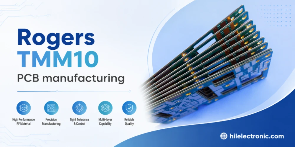
Rogers TMM10 PCB Manufacturing for RF Designs
Table of contentsHow TMM10 Shrinks RF StructuresTMM10 vs...
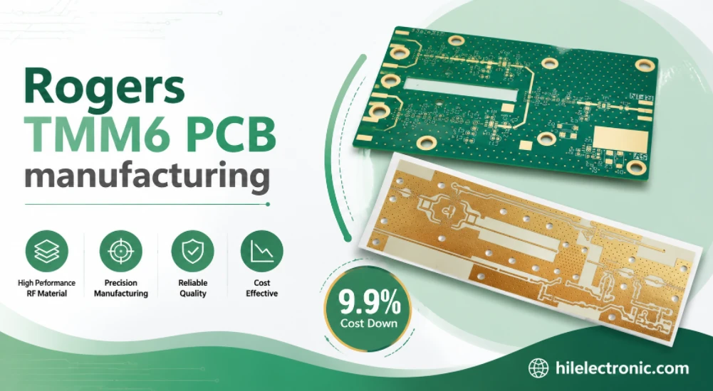
Rogers TMM6 PCB Manufacturing for Microwave Filters
Table of contentsWhy Microwave Filter Designers Use...
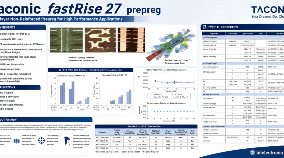
Taconic fastRise 27 Prepreg PCB Bonding and HDI Fabrication Service
Table of contentsWhat fastRise 27 Is—and What You Are...
How to get a quote for PCBs
Let‘s run DFM/DFA analysis for you and get back to you with a report. You can upload your files securely through our website. We require the following information in order to give you a quote:
-
- Gerber, ODB++, or .pcb, spec.
- BOM list if you require assembly
- Quantity
- Turn time
In addition to PCB manufacturing, we offer a comprehensive range of electronic services, including PCB design, PCBA, and turnkey solutions. Whether you need help with prototyping, design verification, component sourcing, or mass production, we provide end-to-end support to ensure your project’s success.
For PCBA services, please provide your BOM (Bill of Materials) and any specific assembly instructions. We also offer DFM/DFA analysis to optimize your designs for manufacturability and assembly, ensuring a smooth production process.