
RF PCB Design Challenges and Solutions for IoT & 5G Devices

Introduction
The proliferation of IoT and 5G devices has fundamentally transformed the electronics landscape. Global IoT connections are projected to exceed 30 billion by 2025, while 5G networks now operate across frequency bands extending from sub-6 GHz to millimeter-wave ranges beyond 24 GHz. This expansion demands RF PCBs capable of handling unprecedented integration complexity within increasingly compact form factors.
RF PCB solutions for IoT and 5G devices require precise material selection, controlled impedance routing, and miniaturized layouts to maintain high-frequency performance and signal integrity. This article explores the key RF PCB design challenges and solutions for modern IoT and 5G devices.
The Role of RF PCBs in IoT and 5G Devices
Core Functions and System Integration
RF PCBs serve as the critical foundation for wireless communication systems, providing the physical infrastructure that connects radio frequency front-end modules, power amplifiers, filters, and antenna interfaces. These boards handle signal transmission and reception while managing impedance matching networks and filtering circuits essential for clean RF performance.
Application-Specific Design Priorities
IoT devices prioritize power efficiency and compact dimensions, typically operating in the sub-6 GHz spectrum with design emphasis on battery longevity and minimal footprint. Conversely, 5G infrastructure and user equipment demand support for wide bandwidths, multi-band operation, and frequencies extending into millimeter-wave territory where signal losses become significantly more pronounced. Across both domains, RF PCB design targets consistent low insertion loss, minimal crosstalk between signal paths, and effective thermal dissipation.
Key RF PCB Design Challenges for High-Frequency Applications
Miniaturization and Layout Density
The drive toward smaller device profiles forces extreme component density on RF PCBs, creating significant electromagnetic coupling challenges. When high-frequency traces run in close proximity, unwanted capacitive and inductive coupling introduces crosstalk that degrades signal quality. Ball grid array and land grid array packages impose strict constraints on routing channels and via placement beneath component footprints.
Designers employ microstrip and stripline configurations strategically to isolate sensitive RF paths. Microstrip lines on outer layers facilitate impedance control, while buried stripline routing between ground planes offers superior isolation for critical signal paths requiring maximum electromagnetic shielding.
High-Frequency Signal Integrity
Operating frequencies above 6 GHz amplify every imperfection in the signal path. Dielectric losses, conductor losses, and impedance discontinuities create dominant factors limiting RF PCB performance in IoT and 5G devices. Material selection proves crucial, as dielectric constant stability directly affects characteristic impedance across temperature and frequency variations.
Advanced design techniques ensure signal integrity:
- Ground via fencing – Electromagnetic barriers along RF transmission lines contain field energy and reduce radiation losses
- Via-in-pad technology – Eliminates stub lengths that introduce resonances and reflections at high frequencies
- Controlled impedance routing – Precise trace geometry accounts for dielectric thickness tolerance and fabrication variations
- Differential signal paths – Balanced layout approaches minimize common-mode noise and electromagnetic interference
Thermal and Mechanical Reliability
Power amplifiers and RF front-end modules generate concentrated heat loads that challenge thermal management in compact assemblies. High-density layouts restrict airflow and reduce convective cooling effectiveness, while stacked components create thermal bottlenecks.
Metal-core PCBs provide direct thermal conduction paths from heat-generating components to external heat sinks. Thermal via arrays placed beneath power devices create low-resistance channels that spread heat into internal copper planes. Mechanical reliability concerns include vibration resistance and dimensional stability, as high-frequency laminates often exhibit different coefficients of thermal expansion compared to standard materials.
Assembly and Component Integration
High-frequency component assembly demands exceptional process control to achieve reliable interconnections. Co-planarity requirements tighten considerably when dealing with fine-pitch ball grid arrays and RF connectors operating at millimeter-wave frequencies. Surface flatness variations can create open circuits or impedance mismatches in RF applications.
Solder paste stencil design requires optimization to deposit precise volumes that prevent bridging while ensuring adequate joint formation. Micro ball grid array packages with pitch dimensions below 0.4 millimeters demand advanced inspection techniques, including automated optical inspection for surface verification and X-ray inspection for hidden solder joint quality validation.

Material and Stack-up Considerations for RF PCB Solutions
High-Frequency Laminate Selection
Material selection forms the foundation of successful RF PCB design for IoT and 5G devices. Rogers 4003C offers balanced electrical performance with dielectric constant of 3.38 and loss tangent of 0.0027 at 10 GHz. Rogers 4350B provides similar performance with compatibility for standard processing equipment, reducing fabrication costs. PTFE-based laminates deliver superior performance with loss tangent values below 0.001.
Liquid crystal polymer materials offer extremely low moisture absorption, stable dielectric properties across wide frequency ranges, and reduced thickness compared to traditional laminates. These characteristics make LCP particularly attractive for millimeter-wave applications and flex-rigid assemblies where dimensional stability proves critical.
Stack-up Architecture Design
Stack-up architecture requires careful planning to optimize both electrical performance and manufacturing yield. A typical configuration places primary RF signal traces on outer layers adjacent to continuous ground planes, providing controlled impedance and minimizing radiation. Buried stripline layers handle sensitive signals requiring maximum isolation.
Hybrid stack-ups combining standard FR4 core layers with high-frequency laminates on outer layers present economical solutions. This approach reserves premium materials for critical RF sections while using cost-effective FR4 for power distribution and digital control circuitry, enabling consistent impedance control for compact IoT and 5G modules.
Practical Manufacturing Solutions for RF PCB Production
Precision Fabrication Processes
Impedance control execution requires rigorous process monitoring and validation. Target impedance values must account for fabrication tolerances, with specifications typically holding trace width and dielectric thickness within plus-or-minus 10 percent. Time-domain reflectometry testing on production coupons verifies impedance consistency before board shipment.
Advanced fabrication capabilities include:
- Precision etching – Controlled photolithography and etchant chemistry produce smooth sidewalls and minimal undercut, reducing conductor losses
- Laser drilling – Creates microvias with diameters below 0.1 millimeters for high-density interconnections
- Copper-filled vias – Eliminates stub resonances and provides robust thermal conduction paths
- Tight tolerance control – Maintains dimensional accuracy critical for millimeter-wave performance
High-Reliability Assembly Processes
High-reliability assembly processes incorporate multiple verification stages for RF PCB solutions. Controlled reflow profiles developed specifically for RF assemblies balance thermal requirements across diverse component types. Automated optical inspection systems verify component placement and solder joint appearance, while X-ray inspection confirms hidden connections beneath area array packages.
Electromagnetic compatibility optimization requires coordinated attention to layout, grounding, and shielding strategies. Continuous ground planes provide low-impedance return paths that minimize loop areas and reduce radiated emissions. Strategic placement of decoupling capacitors maintains clean supply voltages for IoT and 5G devices.
Future Trends in RF PCB Technology
Millimeter-Wave and Antenna Integration
Millimeter-wave technology continues advancing beyond initial 5G deployments, with frequency bands extending to 40 GHz and higher for enhanced bandwidth applications. Antenna-in-package solutions integrate radiating elements directly with RF front-end modules, requiring PCB substrates that support both high-frequency signal routing and antenna performance.
Advanced Material Development
Material science developments focus on ultra-low-loss laminates with dissipation factors below 0.0005 and improved thermal conductivity. Advanced liquid crystal polymer formulations promise thinner dielectric layers while maintaining mechanical robustness. Hybrid substrate technologies combining organic materials with ceramic reinforcements target applications requiring both high-frequency performance and superior thermal management.
The trajectory points toward progressively thinner board constructions with tighter impedance tolerances and reduced conductor losses. Fine-line processing capabilities continue improving, enabling trace widths approaching 25 micrometers for maximum routing density in next-generation RF PCBs for IoT and 5G systems.
Conclusion
RF PCBs represent the essential enabling technology for IoT and 5G wireless systems, translating communication protocols into physical hardware capable of reliable high-frequency signal transmission. The challenges of miniaturization, high-frequency operation, thermal management, and precision assembly require integrated solutions addressing electrical, mechanical, and manufacturing considerations simultaneously.
Highleap Electronics provides comprehensive RF PCB capabilities through advanced manufacturing processes and engineering expertise:
- Precision impedance control – Tolerances meeting millimeter-wave application demands with verified consistency across production
- Advanced thermal management – Metal-core substrates and optimized via structures for concentrated heat dissipation
- High-reliability assembly – Controlled reflow processes, multi-stage inspection protocols, and functional validation testing
- Material expertise – Experience with Rogers laminates, PTFE, LCP, and hybrid stack-up configurations
Ready to advance your RF PCB project? Contact Highleap Electronics to discuss your specific requirements and discover how our manufacturing expertise can accelerate your product development timeline while ensuring superior performance and reliability.

Recommended Posts
Electronic Contract Assembly: Models, Selection, and the Full Build Process
Figure 1. Electronic Contract Assembly reference image for...

How to Clean Flux Off a PCB: The Right Method for Each Flux Type
Figure 1. How To Clean Flux Off Pcb reference image for...
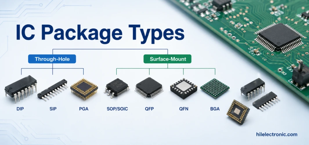
IC Package Types Explained: BGA vs QFN vs QFP, and How to Choose for Your PCB
Figure 1. IC package types image for PCB manufacturing...
Copper Clad Boards (Copper-Clad Laminate): What They Are, Types, and How PCBs Are Made From Them
Figure 1. copper clad boards image for PCB manufacturing...
How to get a quote for PCBs
Let‘s run DFM/DFA analysis for you and get back to you with a report. You can upload your files securely through our website. We require the following information in order to give you a quote:
-
- Gerber, ODB++, or .pcb, spec.
- BOM list if you require assembly
- Quantity
- Turn time
In addition to PCB manufacturing, we offer a comprehensive range of electronic services, including PCB design, PCBA, and turnkey solutions. Whether you need help with prototyping, design verification, component sourcing, or mass production, we provide end-to-end support to ensure your project’s success.
For PCBA services, please provide your BOM (Bill of Materials) and any specific assembly instructions. We also offer DFM/DFA analysis to optimize your designs for manufacturability and assembly, ensuring a smooth production process.