
Portable Radiation Detector PCB: Design, Assembly and Manufacturing Considerations
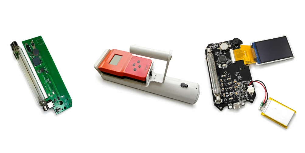
Two handheld radiation instruments can look similar and still require very different PCB manufacturing controls. A Geiger-Müller (GM) tube counter needs a specified high-voltage bias and reliable pulse pickup. A semiconductor instrument may measure extremely small charge or current at a sensitive analog input. A scintillation detector can use a photomultiplier tube (PMT) or silicon photomultiplier (SiPM), each with its own bias and readout requirements. For a portable radiation detector PCB, the detector and its signal chain determine the critical fabrication and assembly work.
Highleap Electronics manufactures customer-released radiation detector PCBs and PCBAs through its electronic manufacturing services. The agreed scope may include PCB fabrication, approved component sourcing, SMT/THT assembly, programming and board-level inspection or functional testing. High-voltage spacing, input leakage, converter noise and the handling of precision components have to be defined in the build documentation—not inferred from the product name.
Board-level electrical checks are not the same as radiation-response calibration. Calibration with suitable radiation sources, dose or dose-rate performance claims and regulatory approval require separately defined procedures and qualified arrangements.
Different Detector Technologies Require Different PCB Assemblies
There is no standard circuit board that serves every handheld radiation detector. Before a manufacturing quotation can accurately cover materials, assembly and test, the OEM needs to identify the sensing element and the electrical interface it actually uses.
| Detector configuration | Electronic interface | What affects the PCBA build |
|---|---|---|
| GM tube counter | Tube bias and pulse discriminator | Voltage-rated parts, HV spacing, detector connector and switching-noise control |
| Semiconductor detector | Detector-specific bias and low-current or charge-sensitive front end | Clean input surfaces, low-leakage components, precision population and specified guarding |
| Scintillation detector | PMT or SiPM bias, amplification and pulse processing | Photosensor interface, gain-stage components, bias requirements and connector integrity |
| Integrated detector module | Specified module supply and digital or analog output | Approved module sourcing, mating connections, mechanical position and programming |
Across these designs, the signal chain typically connects a sensing element to bias and analog signal conditioning, then to pulse counting or digitization and finally to an MCU, display, alarm or logger. Those functions may share one PCB or occupy separate detector, power and interface boards. Neither arrangement should be assumed without a board-set drawing.
Define the detector-to-board boundary before the first build
The RFQ should identify the detector part number or supplied module, its connector and bias requirements, which components the OEM will consign, and whether the sensitive front-end assembly is included. A display, BLE radio, USB port or charger is comparatively straightforward to identify on a BOM; the detector interface is where changing one approved component can alter the measurement electronics.
The manufacturing review of critical PCB features should therefore flag any proposed changes to detector traces, high-voltage spacing, precision parts or test access for engineering approval. Panelization or assembly access can be improved without treating these electrical features as ordinary cosmetic layout details.
Geiger-Müller Detector PCBs and High-Voltage Bias Assembly
A battery-operated GM survey meter may still require several hundred volts at its tube, according to the selected detector’s datasheet. Its boost supply can include a transformer or inductor, switching device, rectification, storage capacitors and high-value feedback or current-limiting components. The actual values, operating region and protection strategy belong to the released OEM design.
Spacing must follow the working voltage and intended environment
There is no single safe creepage or clearance dimension for every radiation detector PCB. Voltage, transients, insulation system, material properties, contamination conditions, altitude and applicable equipment requirements can affect the required distances. The fabrication package should explicitly identify no-copper areas and critical clearances. A high-voltage PCB fabrication review must preserve those approved constraints rather than narrow them to simplify routing.
Keep converter noise out of the pulse-input path
Fast switching current in the bias converter can couple into the pulse-discriminator input, especially when the switching loop and detector wiring are close. The approved board geometry should keep the high-energy loop compact and the sensor input away from it. Return-path and decoupling details also matter: a re-layout that changes converter current paths and power integrity should be reviewed as an electrical change, not just a placement adjustment.
Voltage rating and substitution controls belong in the BOM
The rating of an HV capacitor, diode or resistor is not defined by its footprint. Resistance and capacitance values alone may not establish suitability, and series arrangements can require matched electrical characteristics. Approved part numbers and alternates should be maintained through controlled sourcing of voltage-rated components. Any substitution that changes voltage stress, leakage or timing needs OEM review before the build proceeds.
Where high-voltage output checks are included in production, the approved fixture, safe operating procedure, measurement point and acceptance window need to be defined separately. Such electrical checks do not establish the instrument’s radiation sensitivity or dose-rate calibration.
Low-Noise Analog Front-End Assembly for Radiation Detectors
A semiconductor sensor, GM pulse pickup or scintillation photosensor can deliver a small signal beside a noisy digital and power system. The front-end amplifier, shaping network, comparator or ADC must be assembled with the intended noise, gain and threshold components. A visually sound solder joint does not prove that a high-impedance input remains clean and electrically quiet.
Surface residue can be part of the circuit error
On sensitive nodes, ionic contamination, flux residues, moisture or handling contamination can introduce leakage or drift. The OEM should identify any specified cleaning method, no-clean restrictions, protective materials and permitted handling of the detector module. The correct PCB cleaning and residue-control procedure must be compatible with the assembled parts; aggressive cleaning is not automatically safer for every sensor or connector.
Ground separation should follow return currents
Analog and digital circuitry does not become quieter merely by splitting the ground plane into arbitrary islands. Converter, display and radio return currents should be managed so they do not disturb the detector reference, while sensitive signals retain the intended return path. If the released layout uses guarding, shielding or a particular reference-plane arrangement, the PCB fabricator should reproduce it without informal changes.
Precision resistors, low-leakage capacitors and analog ICs may be selected for characteristics that a nominal-value substitution does not capture. Temperature behavior, dielectric properties, bias current, recovery time and package contamination sensitivity can all matter, depending on the circuit. The approved BOM should distinguish unrestricted alternates from parts requiring engineering sign-off.
Manufacturing Mixed-Signal Detector Boards Without Compromising the Measurement Path
In a compact handheld unit, high-voltage conversion, pulse measurement, MCU clocks, alarms, radio and battery charging may occupy the same small PCB. They do not all demand the same manufacturing controls. The released assembly drawings should make the sensitive interfaces and prohibited changes obvious to the fabrication, sourcing and test teams.
- High-voltage zone: preserve required copper spacing, approved insulating features and the switching-loop geometry. Identify components requiring special handling or inspection.
- Detector input and analog front end: protect high-impedance nets from residue and unnecessary handling; preserve guard patterns and input-component placement where specified.
- MCU and display circuitry: keep the approved reference planes, clock-related routing and return-current paths intact.
- USB, BLE and alarms: reproduce the specified ESD, filtering, antenna and connector arrangements without moving noisy loads toward the analog input.
- Battery and charger: maintain the approved current-carrying connections and power return paths, particularly when charging or alarms operate during measurement.
Layer count is a design decision, not a detector specification
A multilayer PCB can provide continuous reference planes and more routing separation, while a simpler instrument may be built on two layers when the electrical design supports it. Board density, high-voltage geometry, noise margin and enclosure space determine the released construction. A PCB stack-up review should be based on those requirements, not a claim that every radiation detector needs a fixed number of layers.
Some test pads can change what is being measured
On a high-impedance detector node, an added test pad can increase capacitance and provide another surface where leakage may occur. A long test loop beside the HV converter can also pick up switching interference. Where access is needed, the OEM should approve the measurement point, fixture connection and any buffering. Testability improvements should not be introduced by the assembler at the expense of the measurement path.
For a first article, it is useful to document the actual detector module and interface, critical spacing, approved analog component population and access to the agreed electrical test points. That record helps separate a later assembly or sourcing change from a detector-calibration issue without claiming that PCB inspection alone establishes instrument accuracy.
Is the Detector Interface Defined for Your PCB Build?
Send your Gerber files and BOM together with the detector model, bias-voltage limits, sensitive-node handling notes and board-level test requirements. Highleap can discuss PCB fabrication, approved sourcing, assembly and the electrical checks included in your manufacturing order. Radiation-source calibration is quoted only if separately agreed and qualified.
| Get My Quote | Discuss My Build |
PCB Fabrication: Cleanliness, Solder Mask, Finish and Stack-Up
A portable radiation detector PCB may pass bare-board continuity testing yet still have manufacturing-related risks around a high-impedance sensor input or high-voltage bias circuit. An open or short is not the only concern: unintended leakage, altered copper spacing and contamination after assembly can affect the measurement path. The fabrication drawing needs to identify which locations require tighter control than the rest of the board.
Define cleanliness at the sensitive nodes
For a low-current detector front end, an acceptable cleaning process depends on the components, residues, surface geometry and the OEM’s electrical limits. The specification should distinguish bare-board cleanliness from post-soldering PCBA cleanliness; passing one does not establish the other. If a detector module must not be washed or exposed to a particular solvent, the assembly route should identify when it is fitted and which cleaning operations remain permitted.
Areas worth calling out on the drawing include detector-input pads, guard structures, high-value resistor networks, connector pins carrying small signals and any inaccessible spaces where residue could remain. The manufacturer should work to the released contamination or leakage acceptance method rather than apply an arbitrary universal threshold.
Solder mask and surface finish do not replace electrical design rules
Solder mask openings, registration and copper clearance are especially important around high-voltage and high-impedance regions. Solder mask is not automatically a qualified insulation barrier, so the specified creepage, clearance and other safety measures must not depend on it unless the OEM’s insulation design explicitly permits that construction.
ENIG, lead-free HASL or another finish can be appropriate according to pad geometry, soldering needs and the released fabrication specification. None makes a poorly controlled detector input inherently low-noise. Fine-pitch parts, test contacts and connector mating surfaces should drive finish selection, not generic claims about a “medical-grade” or “radiation-grade” PCB.
Quote the actual stack-up, not an assumed layer count
A multilayer board may help maintain reference planes around a processor, analog front end and wireless interface; a simpler counter may be adequately implemented on fewer layers. The PCB supplier needs the actual laminate, thickness, copper weights, spacing constraints and any controlled-impedance requirements. Changing plane arrangements or relocating a high-impedance trace to make production easier should be handled as an OEM engineering change, not a routine fabrication substitution.
Radiation Detector PCBA, Inspection and Rework Control
A radiation detector assembly may contain a fine-pitch MCU, voltage-rated converter components, low-leakage analog parts and a detector connector that is mechanically or electrically sensitive. Those parts do not all benefit from the same inspection or rework method. The build should identify the operations that need different handling before the first production panel reaches the SMT line.
Inspect solder workmanship without confusing it with sensor performance
Automated optical inspection of populated boards can check visible placement, orientation and many solder-joint defects. X-ray inspection may be justified for relevant hidden joints, but should not be presented as necessary for every detector. Neither method proves that a high-impedance input has sufficiently low leakage or that a GM tube counts correctly.
For a first article, the OEM and assembly team should record the approved voltage-rated component population, detector connector seating, permitted cleaning route and firmware identity. A documented first-article assembly reference helps repeat orders preserve details that an ordinary placement photograph can miss.
Decide when the detector module is installed
If a detector or photosensor module is costly, moisture-sensitive or unsuitable for reflow, it may be preferable to electrically screen the underlying PCBA before installing it. That decision needs the module supplier’s handling instructions and an agreed assembly sequence. It should not be assumed that every detector module can be reflowed, cleaned or replaced like an ordinary SMT component.
Rework rules should also identify restricted heating near the detector interface, how residues will be removed or inspected afterward, and whether an affected board requires a repeat leakage or pulse-response check. Uncontrolled manual rework can create a new measurement problem while correcting a visible solder defect.
Program the hardware variant, not just the microcontroller
Two PCBAs can share the same bare board while using different detector modules, bias settings or analog populations. If firmware and production test limits depend on those differences, they need a traceable revision or variant identifier. Calibration constants may also be stored on the board, but they must come from the OEM’s approved process; the assembly factory should not generate or alter radiation calibration data by inference.
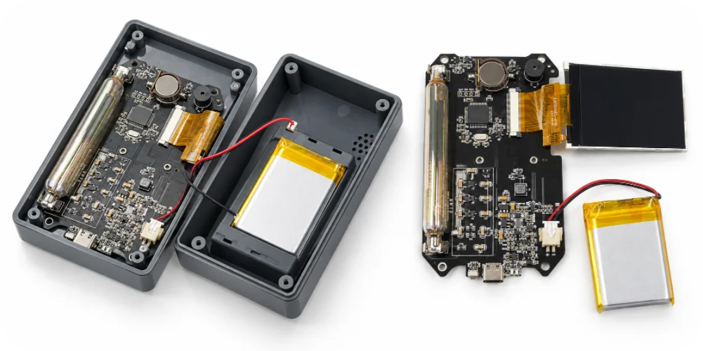
PCB Assembly Testing vs Radiation Instrument Calibration
This distinction should appear in the quotation and in the inspection report. PCBA functional testing checks that the supplied electronic assembly meets agreed electrical and programmed-function limits. Radiation instrument calibration establishes how the finished sensing system responds to a defined radiation field under controlled conditions. Passing the first does not establish the second.
What can be verified at the electronic assembly stage?
The exact test depends on the detector architecture and the fixture provided. A useful customer-defined sequence may cover:
- Power and bias: Check input current, regulated rails and, where applicable, the detector bias output using the specified safe fixture and limits.
- Measurement electronics: Inject a defined electrical pulse or use an approved detector-interface simulator, where the design supports this, to check the pulse-processing chain.
- Firmware and controls: Confirm the required hardware profile, boot behavior, display, alarm, logging or communication features fitted to the board.
- Unit identification: Record the PCB revision, detector variant, firmware version and test result if these records are required for the order.
Highleap can discuss customer-specified electrical and functional tests when fixture access, procedures and pass/fail criteria are agreed. An injected electronic pulse can verify part of the counting chain; it does not validate detector efficiency, dose-rate accuracy or energy response to real radiation.
What needs a separate calibration or qualification process?
Survey meters, personal dosimeters and other radiation instruments can have very different calibration and regulatory requirements. Work involving radiation sources, reference fields, exposure geometry, traceability or formal performance claims requires a separately defined, appropriately qualified process. These activities should not appear in a standard PCBA quotation simply because the board has a detector connector.
If a qualified calibration arrangement is part of the project, the OEM should identify the responsible organization, reference method, equipment, data records and handover point. This keeps the assembly test report distinct from any calibration certificate or product-level approval.
Cost, Prototype Strategy and Production Reliability
On a detector PCBA, the cheapest bare board is not necessarily the lowest-cost production choice. Detector modules, voltage-rated parts, precision amplifiers, controlled cleaning and test fixtures may outweigh modest differences in laminate or layer count. The useful commercial question is which requirements are essential to preserving the approved measurement circuit and which manufacturing operations can be repeated economically.
Use prototypes to expose interference before it looks like a yield problem
An OEM prototype evaluation should compare the measurement chain across the device’s actual modes: display active, alarm operating, charging in progress and wireless transmission if present. Any additional pulses or baseline changes need to be assessed against an agreed electrical reference and test environment. The battery state and high-voltage startup behavior may also need attention for the selected detector architecture.
These investigations establish the OEM’s design and qualification limits. They are not automatically production-line tests; the manufacturer needs a smaller, repeatable acceptance method derived from the approved findings.
Fix the process sequence before repeat orders
The pilot build should establish whether the detector is mounted before or after soldering, what cleaning is permitted, which components cannot be substituted, how each hardware variant is programmed and which test results must be retained. If a unit uses several detector options, a single PCB drawing is insufficient without a variant-specific BOM, firmware image and acceptance profile.
For recurring production, test time and handling often determine cost more than a generic PCB price. A fixture that verifies an agreed bias rail or simulated pulse response can reduce ambiguous manual checks, but the fixture itself requires specification and investment. Highleap can quote manufacturing operations once those responsibilities are defined; it should not claim a particular detector yield or measurement accuracy without project evidence.
What Engineers Should Send to a Radiation Detector PCBA Manufacturer
An RFQ for portable radiation detector PCB manufacturing and assembly should tell the factory which electrical regions require special treatment and which deliverables it is responsible for. Sending Gerber files without detector documentation, handling restrictions or test conditions may be enough to price bare PCB fabrication, but not necessarily a complete assembled and tested board.
A release package that allows a meaningful quote
- Fabrication files: Gerber/ODB++, layer stack-up, board drawing and marked high-voltage or high-impedance regions, including any special cleanliness or spacing criteria.
- Assembly data: Approved BOM, placement files, assembly drawings, critical-component alternates, detector connector details and permitted rework/cleaning instructions.
- Detector interface: Tube, semiconductor sensor, scintillation module or integrated-module identification, datasheet, bias requirements and whether the OEM supplies the detector.
- Firmware and variants: Programming image, hardware-to-detector configuration map and requirements for serial number or per-unit data handling.
- Test boundary: Electrical fixture or simulator, bias and pulse-response limits, inspection records and the party responsible for any separate radiation calibration.
- Order scope: Prototype and expected production quantities, board count per instrument, consigned components, delivery requirements and whether post-PCBA module fitting is included.
These details let Highleap distinguish a controller-board order from a sensitive detector-front-end PCBA with additional handling and fixture work. When approved material purchasing, fabrication and population need to be coordinated, the OEM can request an agreed turnkey fabrication and component assembly scope rather than an undefined finished-instrument price.
For an initial quote: provide the files already released and identify the detector or test details still awaiting approval. A manufacturing scope can then be discussed without treating unfinished calibration or product qualification as included PCBA work.
Frequently Asked Questions
Can a detector PCB be functionally tested without a radiation source?
Often, yes, for specified electronic functions. Depending on the circuit, a fixture may check power rails, detector bias, counting logic and response to an injected electrical pulse. Such a test does not establish response to radiation or a calibrated dose-rate reading.
Should the detector be installed during SMT assembly?
That depends on the detector or module datasheet and the approved process. Some parts can be assembled with conventional electronic components; others require protected handling or installation after reflow and cleaning. The OEM should specify whether the detector is supplied separately and when it may be mounted.
Why can a PCB pass inspection and still show unstable readings?
Visual or X-ray inspection cannot detect every leakage, interference or firmware-configuration problem. Residues near a high-impedance input, coupling from the converter or the wrong hardware profile are possible investigation paths. The actual cause must be established against the released circuit and controlled test setup.
Do all handheld radiation detectors require high-voltage PCBs?
No. A GM-tube design commonly has a high-voltage bias requirement, but semiconductor and scintillation detector architectures vary. The selected sensing device determines whether high voltage is needed and what additional low-noise circuitry or module interface is required.
What should Highleap be asked to quote separately?
Identify any consigned detector modules, custom functional-test fixtures, specialist cleaning or handling, post-assembly module installation, and calibration or certification outside ordinary PCB/PCBA manufacture. That distinction makes quotations and acceptance responsibilities clearer.
PCB manufacturing, assembly and test requirements are confirmed against the released design, component supplier instructions and any applicable end-product qualification requirements.

Recommended Posts
Wearable Haptic Vest PCB Manufacturing & Assembly for Multi-Zone Haptic OEMs
In a wearable haptic vest, the wearer notices the...
Wearable Temperature Logger PCB Manufacturing & Assembly for BLE Sensor OEMs
A wearable temperature logger PCB is the electronic board...
Connected Safety Helmet PCB Manufacturing & Assembly for Industrial IoT OEMs
A Connected Safety Helmet PCB is an industrial IoT...
Mobile Wi-Fi Router PCB Manufacturing & Assembly for 4G/5G Hotspot OEMs
A Mobile Wi-Fi Router PCB is the production platform...
How to get a quote for PCBs
Let’s run DFM/DFA analysis for you and get back to you with a report. You can upload your files securely through our website. We require the following information in order to give you a quote:
-
- Gerber, ODB++, or .pcb, spec.
- BOM list if you require assembly
- Quantity
- Turn time
For PCBA services, please provide your BOM (Bill of Materials) and any specific assembly instructions. We also offer DFM/DFA analysis to optimize your designs for manufacturability and assembly, ensuring a smooth production process.