
Optical Transceiver PCB Manufacturing in China
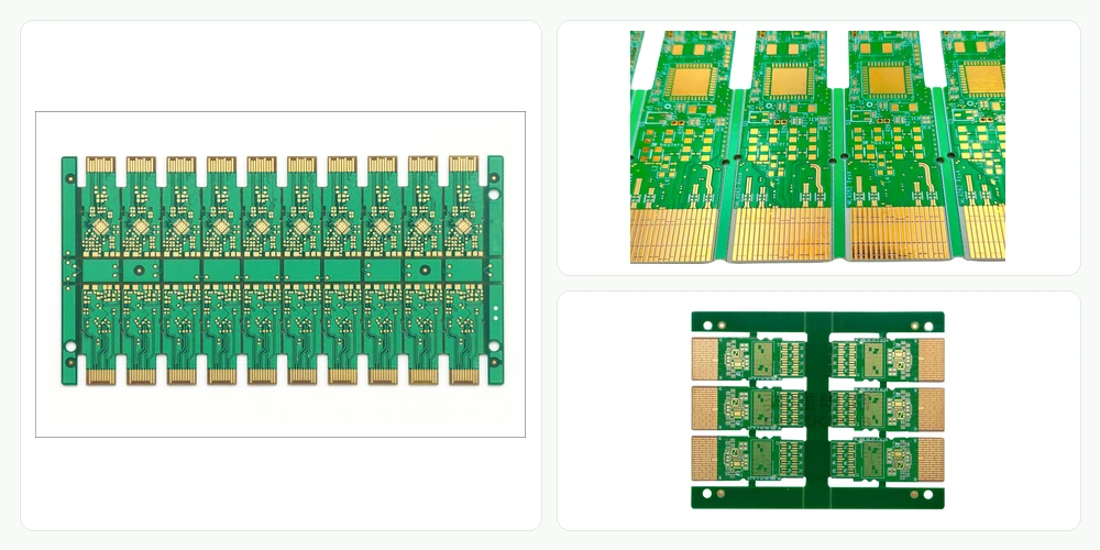
Highleap Electronics provides optical transceiver PCB manufacturing in China for OEM module suppliers and electronics manufacturers requiring controlled multilayer fabrication, compact HDI boards and repeatable production of customer-defined optical-transceiver PCBs. Our bare-board service covers CAM/DFM engineering review, approved material procurement, multilayer lamination, fine-line imaging, drilling and plating, surface finishing, electrical testing and agreed production inspection.
Manufacturing an optical-transceiver PCB is not simply a matter of meeting a layer count. A board may require thin finished thickness, low-loss material, controlled impedance, small vias, selective hard-gold contacts, fine-pitch solder pads and a tightly routed outline in the same design. Highleap evaluates these requirements together before accepting the production route. Customers receive a quotation based on the specified features and inspection scope, rather than an assumption that every “high-speed PCB” uses the same process.
We support prototype orders, pilot builds and recurring production. Submit the released stackup, fabrication data, drawing, material and finish notes, quantity and requested date so our engineering and manufacturing teams can assess the actual board.
Table of contents
- Engineering Review Before Optical Transceiver PCB Production
- Low-Loss Material Procurement and Multilayer Lamination
- Fine-Line Etching, Mechanical Drilling and HDI Processes
- Selective Plating, Gold Fingers and Finished-Board Geometry
- Inspection, First Articles and Production Process Control
- Optical Transceiver PCB Fabrication Quotes and Production Orders
BARE-BOARD MANUFACTURING
Request a Manufacturing Feasibility Review
Provide your Gerber/ODB++ data, stackup, via drawings, finishes, quantities and acceptance requirements.
Request a PCB Fabrication Quote →Engineering Review Before Optical Transceiver PCB Production
Highleap starts optical transceiver bare-board manufacturing with a controlled engineering review of the released design package. CAM artwork, drill data, material schedule, via map, stackup, board outline, surface-finish requirements and acceptance criteria must describe the same board. A quote based only on the number of layers, board size and a few minimum dimensions cannot establish whether the actual build is ready for stable fabrication.
An engineering review also separates the features that are normally covered by the chosen manufacturing process from those needing a special operation or exception. The purpose is to avoid discovering a hard-gold contact, filled-and-capped BGA via, hybrid laminate or unusually tight tolerance only after the purchase order has been accepted. Potentially conflicting documents are clarified before the production route and commercial terms are finalized.
Essential CAM and DFM Release Checks
-
File revision reconciliation: Gerber or ODB++ layers, NC drills, slots, rout paths, fabrication notes and drawing revision are checked for consistency. A contact finish shown only in a mechanical drawing or a via structure missing from the drill map can cause a major processing error. Conflicting information is returned to the design owner rather than resolved by an unrecorded manufacturing assumption.
-
Material and stackup confirmation: Laminate grade, dielectric construction, copper weight by layer, final board thickness and approved alternatives are assessed together. Particular low-loss or hybrid materials may need dedicated pressing conditions or procurement lead time. A general instruction to “use high-speed FR-4” is not the same as a qualified material baseline, especially for a previously validated customer channel.
-
Manufacturing feature combination: Minimum trace/space, annular ring, drill diameter, hole-to-unconnected-copper clearance, copper thickness and registration are evaluated as a combination. A shop’s smallest advertised trace or tool size is not proof that the entire design can be built economically at those limits. If the process margin is narrow, the exception and any proposed alternative are documented for customer review.
-
Via-treatment and HDI definitions: Blind and buried interconnections require a layer-connection map and appropriate lamination plan. If via-in-pad is present, the drawings must specify whether filling, planarization and copper capping are required; ordinary solder-mask plugging cannot be assumed equivalent under a fine-pitch solderable pad. These operations affect price, inspection and lead time and therefore belong in the original quotation.
-
Critical contact and mechanical dimensions: The edge-contact area, finish, plated thickness where specified, beveling, outline and module-fit dimensions are reviewed against the customer’s released drawings. ENIG pads and selective hard-gold wear contacts have different fabrication requirements. The accepted inspection method and any controlled connector datums are established before production.
-
Acceptance and delivery prerequisites: Electrical test, impedance verification, microsections, material traceability, dimensional records and any customer-defined reliability report are agreed by scope, method and sampling. Neither a generic statement of “100% testing” nor an approved CAM file substitutes for the required acceptance evidence. The production lead-time commitment should start from an explicitly agreed release milestone.
Resolve the Engineering Exceptions Before Tooling
Highleap’s PCB DFM review can identify those gaps before fabrication starts. The outcome is a defined manufacturing package, confirmed technical exceptions and an RFQ based on the actual design. Customer approval is obtained for any change that affects copper artwork, impedance, material performance, connector fit or reliability; an improved factory yield is not a reason to alter released product requirements silently.
Low-Loss Material Procurement and Multilayer Lamination
Highleap manufactures optical-transceiver PCBs using the approved rigid laminate system, with high-speed/low-loss grades and hybrid arrangements evaluated according to the design. The customer-specified laminate family, copper foil type, core/prepreg combination and final dielectric thickness control how we establish the material and lamination route. The material choice is not casually replaced with a cheaper FR-4 grade when it forms part of the approved electrical construction.
Specialist materials can require different storage, handling, press cycles and bonding conditions from conventional constructions. Mixing dielectric systems adds another layer of process review: the materials must be compatible with the selected bonding arrangement and required thermal/mechanical behavior. Highleap checks procurement availability and the proposed build sequence before confirming the delivery schedule, especially when a customer requires a named laminate or does not permit substitutions.
Copper distribution and layer construction are also evaluated for registration and dimensional stability. Thin transceiver boards can be sensitive to panel handling and thickness tolerances. Dense internal patterns may create etching and lamination challenges when combined with specialty copper weights. These are addressed through production tooling and process planning, not by promising that every feature will automatically be produced at its isolated capability limit.
Where impedance is specified, the stackup and finished conductor geometry are treated as a coordinated requirement. Approved coupons, measurement tolerance and reporting scope are confirmed in the manufacturing documentation. Highleap’s high-speed PCB material manufacturing resources provide related background on material and build options.
Controlling the Layer Build From Material Issue to Lamination
The approved stackup drives material purchasing, inner-layer preparation and lamination. For transceiver programs using low-loss or hybrid laminates, Highleap checks the laminate and bondply grades, available core/prepreg thicknesses, copper foil type and material compatibility with the requested process. Inner layers are fabricated and inspected before lamination; once embedded, many line and space defects are difficult to recover. A controlled stackup includes the required dielectric spacing, finished copper weights, final thickness and registration allowances, not merely the brand name of the laminate.
A hybrid stack may combine materials with different thermal and dimensional behavior. Lamination parameters and material compatibility therefore need project-specific confirmation. When a requested grade is unavailable, a proposed substitute must be presented against the approved electrical and reliability requirements before any order is changed. Highleap does not treat a lower-cost generic dielectric as an automatic replacement for a customer-qualified high-speed channel construction.
What Changes Between Prototype and Production Lamination
A prototype may be manufactured with readily available panel material or a particular stackup compromise approved for evaluation. Repeat production needs stable supply and a repeatable registered build. We review panel formats, layer registration, material batch documentation where specified and the customer’s restrictions on alternates. If the product requires impedance or thickness reports, the inspection method is incorporated into the build plan. Dedicated insertion-loss verification is specified separately; an impedance result is not a blanket guarantee of module-system performance.
Fine-Line Etching, Mechanical Drilling and HDI Processes
Manufacturing high-density optical transceiver PCBs means controlling more than the headline minimum trace and drill capability. Very fine copper patterns, multiple via architectures and narrow internal clearances may all appear in the same small board. Their combined impact on imaging, etching, drilling, plating, lamination and inspection determines actual manufacturability, yield and the appropriate production route.
Highleap evaluates the intended finished conductor and hole geometry against copper weights, board thickness, layer registration and the specified material system. A feature that can be produced during a specialized trial is not necessarily the best default for recurring volume production. Engineering review focuses on achieving the customer-released electrical and mechanical construction with repeatable process margins and a clear exception procedure.
Key Fabrication Controls for Fine-Line and HDI Transceiver PCBs
-
Artwork compensation and trace profile: Trace width and spacing are reviewed against base foil, final copper, plating strategy and the selected etching process. Fine 2/2 mil routing may need tighter control and additional screening, especially on specialty materials. The factory should not arbitrarily widen an impedance-controlled net; where a less demanding layout is possible, it is proposed to the customer before data release.
-
Drill-tool size versus finished holes: Mechanical drill diameter, finished plated-hole dimensions, tool wear, board thickness and drill count are considered together. A 0.20 mm tool may be feasible but slower and less forgiving than a larger tool in a particular construction. A 0.30 mm drill may reduce manufacturing pressure only when pad sizes, electrical spacing and plating requirements permit it; such changes are never automatic.
-
Hole-to-copper and layer registration: A hole can meet its nominal diameter yet compromise an adjacent internal trace if drilling and layer registration tolerances consume the available margin. CAM checks nonfunctional copper clearances, annular rings, hole-to-hole spacing and the proposed finished thickness. Tight internal gaps may require a revised clearance or approved artwork change rather than simply a different drilling program.
-
Through-hole metallization and inspection: Desmear, deposition and plated copper integrity matter for multilayer electrical continuity and long-term reliability. The accepted process and inspection plan are selected for the actual board construction and hole geometry. Finished-board continuity/isolation tests cannot alone establish plated-barrel wall quality; cross-sections or additional evidence should be included when specified by the customer.
-
HDI sequencing, microvias and via-in-pad: Each microvia or buried connection is tied to its layer pair and lamination stage. Stacked structures, resin-filled and capped vias, and backdrilled holes are different features with different production operations. For solderable BGA via-in-pad, flatness and capping requirements are confirmed with assembly; solder-mask tenting is not treated as a universal substitute for a plated, planar pad.
-
Intermediate defect containment: Inner-layer inspection can catch imaging defects before lamination; subsequent controls address drilling, plating, outer-layer circuitry and final dimensions. If a defect is found, the lot is evaluated against the agreed acceptance criteria and the affected process records—not simply passed because the final electrical test is acceptable. The customer must approve any disposition outside the released specification.
Reconcile Fabrication Difficulty With Volume Production
Detailed process options are described under HDI PCB manufacturing. The relevant manufacturing question for an optical transceiver order is whether the combined stackup, copper geometry and via design can be held consistently at the required quantity and inspection level. This provides a more dependable quotation than treating a laboratory-scale feature demonstration as a blanket production guarantee.
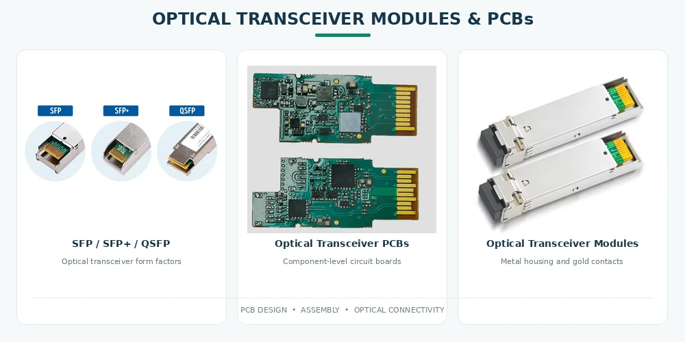
Optical transceiver board and module housing interface examples
Selective Plating, Gold Fingers and Finished-Board Geometry
Many pluggable transceiver boards rely on finished gold-contact geometry that must mate with a host connector. Highleap manufactures to the customer-specified contact and outline requirements, including selective plating, edge-bevel or tight board-thickness features where feasible. The contact finish must be defined accurately: ENIG on component soldering pads does not automatically satisfy a hard-gold wear-contact specification.
The plating requirement should identify the intended hard-gold area, nickel/gold thickness where specified, masking boundaries and any special contact configuration. The process plan also accounts for the relationship between plating, board routing and beveling. Plated contacts at the insertion edge may require more control than a general surface-finish line item conveys; missing details are a common cause of re-quoting after CAM review.
Other precision features may include thin board profiles, castellated edges where specified, routed openings and tightly controlled dimensions around the connector or housing interface. Highleap reviews these with the supplied mechanical reference and fabrication drawing. A board that is electrically sound but misfits the enclosure is a nonconforming product, so the critical dimensions and measurement requirements are confirmed before repeat manufacture.
Surface finish selection also affects subsequent SMT assembly. Special pads or thermal features can require finish and via-treatment choices that should be checked against the assembler’s process. When Highleap supplies both fabrication and assembly, these handoff details are coordinated across the two scopes, with the separate transceiver PCB assembly service available for populated board orders.
Separate Processes for SMT Pads and Contact Fingers
Optical transceiver boards often combine fine-pitch solderable pads with card-edge insertion contacts. The first may require ENIG or another approved finish; the second may call for selective hard gold, a nickel underlayer and a specified contact thickness. Highleap reviews the exact plating area, exclusion masks, edge bevel, conductor-to-edge clearance and inspection method. A drawing that simply says “gold plating” cannot distinguish these requirements and may cause re-quoting after CAM review.
Routing Thin Boards Without Losing Interface Accuracy
A narrow module outline can be sensitive to mechanical routing, panel support and thickness variation. The finished board may need a controlled insertion edge and local flatness beneath components or mating features. Highleap evaluates tooling margins, outline datums, board thickness and measurement needs before panel release. Selective contact plating may impose additional constraints on how the panel is processed, so the finish and outline should be reviewed together rather than as separate items.
Inspection, First Articles and Production Process Control
Highleap’s manufacturing process can include inner-layer and final AOI, plated-hole verification, finished-board electrical testing, critical dimensional inspection and additional customer-specified controls. A production acceptance plan for an optical-transceiver board may also require impedance coupons, microsection records, material traceability, thickness reports or selective plating measurements. These must be defined by the approved drawings and quality agreement; we do not claim that one standard inspection package covers every possible optical-module requirement.
| Manufacturing concern | Verification that can be specified | What the result establishes |
|---|---|---|
| Copper patterns and layer registration | AOI and in-process checks | Identifies defined pattern and alignment defects |
| Plated holes and vias | Electrical testing, cross-section or specified plating inspection | Supports hole and interconnection acceptance against agreed criteria |
| Controlled-impedance structures | Test coupons and documented measurement | Verifies coupon impedance within the agreed test conditions |
| Gold contacts and finished outline | Plating and dimensional inspection | Checks critical contact and mechanical features |
| Repeat batches | Revision, material and lot records | Supports consistent manufacturing scope and traceability |
An impedance coupon result is not the same as a complete channel-loss qualification, and a bare-board E-test does not prove optical performance. Those tests are defined at a different product level. The value of the manufacturing records is that they show whether Highleap fabricated the board to the properties specified for that production lot.
For prototype qualification, we identify which characteristics need first-article evidence and which can follow routine lot inspection. On repeat orders, changes involving laminate, foil, via process, surface finish or critical tooling should be reviewed against the customer-approved production configuration. Our PCB electrical testing resources discuss one part of that bare-board acceptance process.
Layered Verification Rather Than a Single Final Test
Production quality begins before final E-test. Depending on the accepted work scope, inner-layer AOI checks the artwork, drilling and plating controls address plated-hole integrity, visual and dimensional inspection verify the board outline and finish, and electrical testing addresses continuity/isolation. Impedance coupons, cross-sections, thickness measurements and plating verification are performed according to the customer’s ordered criteria. The verification set is chosen to match the actual risk: a card-edge contact program needs different evidence from a standard non-pluggable signal board.
Corrective Actions and Lot Consistency
A prototype that passes a functional evaluation is not enough to permit unannounced changes in laminate, copper profile, via processing or selective plating on later batches. Highleap uses revision and specification controls to compare repeat orders with the released baseline. When a tolerance or special process is unclear, the issue is raised before production; when inspection identifies a nonconforming feature, disposition follows the agreed acceptance criteria and any customer approval requirement. This creates traceable decisions instead of silently shipping a substitute construction.
Optical Transceiver PCB Fabrication Quotes and Production Orders
To request a manufacturing quote, provide controlled Gerber or ODB++ data, NC drill and rout data, layer stackup, laminate grade and dielectric requirements, finished board thickness, copper weights, impedance notes, mechanical dimensions and surface-finish specification. Identify plated or laser-drilled vias, any backdrill or via-stub limits, via-in-pad filling/capping, selective hard gold, edge bevel and other special features. State quantity breaks, expected annual volume, inspection reports and the required delivery target.
Production-Ready RFQ Sequence
- Submit the complete released artwork, drill files, stackup, material grades and contact-finish drawing.
- Identify the special-process items needing engineering approval and any mandatory inspection evidence.
- Request a documented review of exceptions before accepting final cost and production lead time.
- Issue the approved revision and quantity schedule to establish the production baseline.
Highleap reviews the requirements before confirming the fabrication route, material sourcing, technical exceptions, unit price and schedule. A quote may be budgetary while engineering data are incomplete; the approved production quotation reflects the final manufacturing specification. If a mandatory feature exceeds the verified process window, we discuss a technically approved alternative or identify the issue before committing to the order.
Highleap offers bare PCB fabrication as a defined manufacturing scope. Projects needing component procurement, SMT placement or board-level test can be quoted separately as optical transceiver PCB assembly, while our custom transceiver PCB supply also covers module-form-factor and connector-interface requirements. Send your manufacturing files to Highleap Electronics for an engineering-reviewed quotation and production plan.
How the Fabrication Price Is Built
The bare-board quote considers material and panel consumption, number of inner-layer processes, drilling and plating complexity, fine-line constraints, special finishes, ordered verification and quantities. Additional build-up steps, filled vias, controlled-depth drilling or selective hard gold can change both price and capacity. Quick-turn requests must be evaluated against the real process sequence; curing, lamination and plating cannot always be shortened without changing the risk profile.
Include any demanded inspection documentation in the original RFQ. A request for impedance reports, material traceability or critical contact dimensions after the order is placed may introduce extra measurements and scheduling changes. Highleap can distinguish standard fabrication, engineering-reviewed special processes and any separately quoted testing so purchasing can compare the actual accepted scope.
BARE-BOARD MANUFACTURING
Request a Manufacturing Feasibility Review
Provide your Gerber/ODB++ data, stackup, via drawings, finishes, quantities and acceptance requirements.
Pricing, process and schedule are confirmed after engineering review.

Recommended Posts
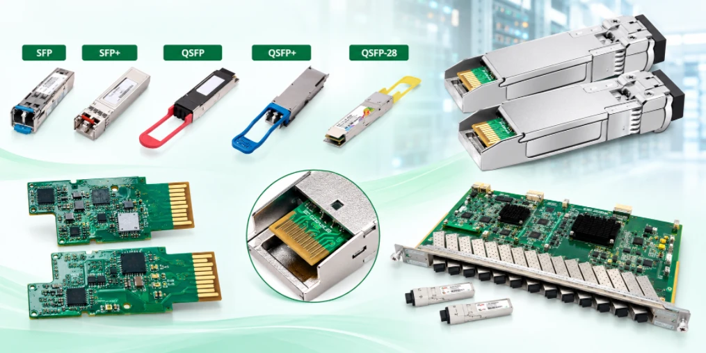
Optical Transceiver PCB Assembly Services in China
Highleap Electronics provides optical transceiver PCB...
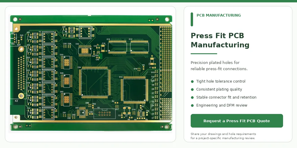
Precision Press Fit PCB Manufacturing with Tight Tolerances
Press-fit PCB manufacturing requires close coordination...
8 Layer HDI PCB Manufacturer in China
Highleap Electronics provides 8 layer HDI PCB...
8 Layer Rigid-Flex PCB Manufacturing and Cost Guide
An 8 layer rigid-flex PCB combines multilayer rigid...
How to get a quote for PCBs
Let‘s run DFM/DFA analysis for you and get back to you with a report. You can upload your files securely through our website. We require the following information in order to give you a quote:
-
- Gerber, ODB++, or .pcb, spec.
- BOM list if you require assembly
- Quantity
- Turn time
In addition to PCB manufacturing, we offer a comprehensive range of electronic services, including PCB design, PCBA, and turnkey solutions. Whether you need help with prototyping, design verification, component sourcing, or mass production, we provide end-to-end support to ensure your project’s success.
For PCBA services, please provide your BOM (Bill of Materials) and any specific assembly instructions. We also offer DFM/DFA analysis to optimize your designs for manufacturability and assembly, ensuring a smooth production process.