
ITEQ IT-170GRA2 PCB: Stack-Up Design and Signal Loss Testing
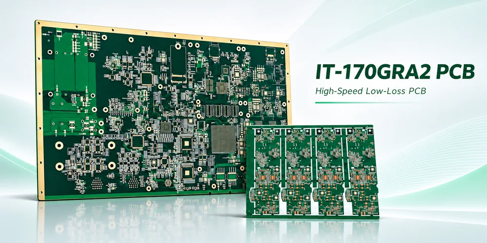
Illustration of high-speed PCB layouts.
ITEQ IT-170GRA2 is a halogen-free, high-Tg epoxy laminate and prepreg for lower-loss multilayer PCBs. ITEQ reports a dielectric constant (Dk) of 3.8 and a dissipation factor (Df) of 0.0080 at 10 GHz on a 50% resin-content specimen. That is a useful starting point for selecting a server, storage, networking or backplane stack-up. The decision to use it belongs to the channel loss budget.
Give the PCB its share of the channel loss budget
Start with a frequency-dependent limit and define the electrical reference planes. If the limit is specified from transmitter package to receiver package, reserve margin for the packages, connectors, launches, via transitions and fabrication variation before assigning the remaining loss to routed board traces. For a simple NRZ link, half the bit rate is the Nyquist frequency; for a multilevel link, use the symbol rate and the applicable specification. A single Nyquist checkpoint is useful for screening, but a production mask may cover a band and include return loss, crosstalk or mode conversion as separate requirements.
A first-pass loss allocation can add estimated positive loss contributions in decibels when the sections are well matched. Then cascade the actual transition and line models or measure the representative channel. Reflections can make the insertion-loss curve ripple, so the arithmetic budget is not a substitute for the cascaded result. Decide early which transitions belong to the board supplier’s test and which must wait until connectors or components are populated.
Compare the longest routed layer segments first. Where the dominant loss is in a long uniform trace, a lower-Df construction and a suitable foil may buy more margin. A short path with a deep plated via stub or a poorly referenced connector launch may benefit more from a layout change. In that second case, putting IT-170GRA2 into the same artwork may leave the main loss mechanism in place.
IT-170GRA2 Dk and Df by frequency
Use IT-170GRA2TC as the laminate designation and IT-170GRA2BS as the prepreg designation when reconciling the drawing with ITEQ’s data. ITEQ lists Tg as 175°C by DSC and 170°C by TMA. Neither value replaces component and solder-paste limits for assembly.
| Frequency | Dk | Df | IPC-TM-650 method |
|---|---|---|---|
| 1 GHz | 4.0 | 0.0060 | 2.5.5.9 |
| 2 GHz | 3.9 | 0.0063 | 2.5.5.13 |
| 5 GHz | 3.9 | 0.0075 | 2.5.5.13 |
| 10 GHz | 3.8 | 0.0080 | 2.5.5.13 |
Source: ITEQ IT-170GRA2 datasheet, Rev. 1.0-26. The frequency points report test results; the table does not define a frequency limit for a product or a guaranteed loss per unit length.
How does it compare with IT-170GT? ITEQ reports 0.0095 Df at 10 GHz and 55% resin content for IT-170GT. The listed values point toward IT-170GRA2 when dielectric loss is the primary concern. They come from different resin contents, so applying the percentage difference directly to a finished channel would be misleading. Recalculate impedance and insertion loss for the proposed glass, pressed thickness and foil before approving a substitution.
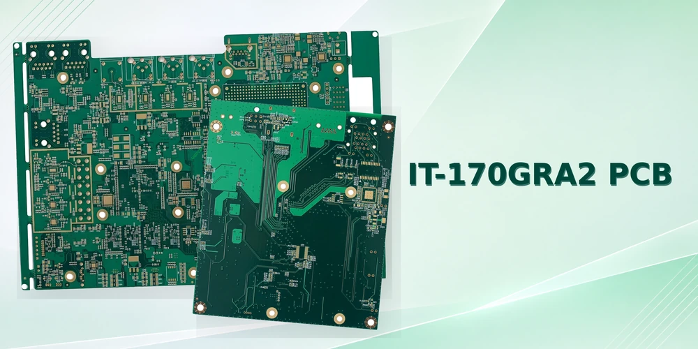
High-speed routing illustration. Evaluate channel loss on the specified stack-up and transitions.
Control the fabrication variables in the field model
Specify the copper surface that faces the dielectric
The smoothness of a foil label alone does not define conductor loss. The bonding treatment and roughness on the relevant copper surface change the current path when skin effect becomes significant. ITEQ’s sheet reports peel strength for a 35 µm low-profile foil reference; peel strength cannot be converted to the roughness parameters needed by a channel solver. Freeze the foil designation and treatment for the signal layer and its reference as applicable, and request roughness information compatible with the solver model. A change in PCB copper roughness can move the loss curve while an impedance coupon still passes.
Keep the line and the discontinuities in the same release
Give CAM an impedance table by layer and reference plane, with finished copper thickness, pressed dielectric, differential gap and allowed artwork adjustments. The etched trace is often trapezoidal; the top and bottom widths need not match the artwork or each other. When there is controlled impedance, a coupon should reproduce the relevant trace geometry and build. A long differential path can also see skew from local glass weave and routing orientation even when the average Dk and impedance look acceptable.
At the layer transition, evaluate the return-path change and the unused via barrel. A poorly placed return via or plane opening changes the transition; a stub can create a frequency-selective notch. Where backdrilling is contemplated, state the signal layer that must be protected, permissible residual stub and depth reference. Check these against both electrical sensitivity and the drill-depth tolerances agreed for the board.
PCB FABRICATION & ASSEMBLY
Planning an IT-170GRA2 PCB build?
Highleap can review the board construction and assembly requirements together.
Include the target impedance, channel loss budget, reference test frequencies and any specified foil.
Measure uniform trace loss separately from launches
Use TDR to locate impedance changes and confirm the line impedance profile. Use a calibrated VNA and an agreed S-parameter measurement to check insertion loss. For a differential line that may be mixed-mode Sdd21; agree on port mapping, normalization, calibration, de-embedding and the reference planes. Differences in launch layout or fixture handling can consume a significant fraction of a short coupon’s measured loss.
Hypothetical coupon calculation. At 10 GHz, a 50 mm trace coupon shows 1.4 dB of positive insertion loss and a 150 mm coupon shows 3.0 dB. With otherwise identical launches and matched uniform lines, the difference suggests about 1.6 dB per 100 mm for that construction at that frequency. Mismatches and fixture asymmetry can invalidate a simple subtraction, so compare the full traces and use the agreed extraction method. These values illustrate the calculation and do not describe an IT-170GRA2 test.
A line-loss coupon includes dielectric and conductor effects together. It does not isolate the resin’s Df, cover every routed layer or reproduce connector and via transitions unless those structures are deliberately included. For a failing first article, use time-domain localization and frequency-domain data together: broad excess attenuation along a uniform length points toward geometry or losses in the construction; a localized reflection or notch calls for checking the launch, return path or via. Neither symptom alone identifies a root cause.
Specify the bare-board and populated tests at quotation
Send the proposed stack-up, routed layer lengths, loss mask, impedance targets, foil requirements, coupon drawings and the electrical reference planes with your Highleap PCB fabrication and assembly inquiry. If the final channel includes populated connectors, add their part numbers, footprints, assembly requirements and any final-fixture definition. Highleap Electronics can review the fabrication inputs, quote assembly against the approved BOM and clarify which measurements belong at first article, at board release or after assembly. Confirm material availability and the measurement scope for the actual build before the design is frozen.

About the Author
Helen Chong
PCB Solutions Consultant & Overseas Business Development Manager at Highleap Electronics
Helen supports international engineering teams with end-to-end PCB fabrication and assembly solutions, helping projects move from quick-turn prototypes to stable mass production. Her experience spans high-frequency and RF boards, complex multilayer stackups, rigid-flex, and flex PCB technologies across multiple industries.
By translating technical requirements into practical manufacturing plans, she helps customers improve manufacturability, reduce risk, and optimize cost and lead time—while maintaining consistent quality at scale.

Recommended Posts
IT-858G Automotive PCBs for Heavy-Copper Power Control
IT-858G PCB applications in automotive electronics and...
IT-958G PCB for High Speed Servers and Backplanes
IT-958G multilayer PCB examples for server and high-speed...
IT-968GSE PCB for High-Speed Networking
IT-968GSE PCB illustration for ultra-low-loss switch and...
Building IT-602G HDI Boards for SSDs and Memory Modules
IT-602G PCB examples for HDI, SSD and memory-module...
How to get a quote for PCBs
Let‘s run DFM/DFA analysis for you and get back to you with a report. You can upload your files securely through our website. We require the following information in order to give you a quote:
-
- Gerber, ODB++, or .pcb, spec.
- BOM list if you require assembly
- Quantity
- Turn time
In addition to PCB manufacturing, we offer a comprehensive range of electronic services, including PCB design, PCBA, and turnkey solutions. Whether you need help with prototyping, design verification, component sourcing, or mass production, we provide end-to-end support to ensure your project’s success.
For PCBA services, please provide your BOM (Bill of Materials) and any specific assembly instructions. We also offer DFM/DFA analysis to optimize your designs for manufacturability and assembly, ensuring a smooth production process.