
Ceramic PCB Cost: A Complete Guide to Pricing Factors and Optimization Strategies

Introduction
Understanding ceramic PCB cost is essential for purchasing managers, design engineers, and procurement professionals who specify high-performance circuit boards for demanding applications. Unlike conventional FR-4 boards, ceramic PCBs command premium pricing due to specialized materials, high-temperature processing requirements, and sophisticated manufacturing techniques that standard organic boards never encounter.
This guide examines 5 primary cost drivers:
- Substrate material selection
- Board complexity including thickness and layer count
- metallization and via processing methods
- production volume and scheduling constraints
- comprehensive testing and qualification requirements
Each factor interacts with the others to create a total cost picture that can vary by an order of magnitude depending on specification choices and volume commitments.
Understanding the Ceramic PCB Cost Model
Fixed Versus Variable Cost Components
Ceramic PCB pricing divides into fixed costs including tooling, screen fabrication, and non-recurring engineering expenses, and variable costs that scale with production volume such as raw substrate materials, metallization consumables, processing time, and per-board inspection. Fixed costs remain constant regardless of order quantity and create significant per-unit overhead for small batches, while variable costs include materials like silver paste or plating chemistry, firing and drilling operations, and testing procedures that accumulate with each additional unit produced.
Primary Cost Buckets
The ceramic substrate cost structure organizes into five distinct categories: material costs reflecting raw substrate type and board dimensions, processing costs from metallization technique and thermal cycles, complexity costs driven by layer count and feature density, yield and testing costs for quality assurance and defect management, and volume costs encompassing production scale and logistics considerations. The prototyping penalty proves particularly significant, where development quantities of five to twenty pieces often carry per-unit costs five to ten times higher than production runs of several hundred units due to setup-intensive processes that only become efficient at scale.

1. Materials: Substrate Choices and Their Impact on Ceramic PCB Cost
Alumina: The Cost-Effective Baseline
Alumina delivers thermal conductivity around 20-30 W/mK with dielectric constants of 9-10 at radio frequencies, breakdown voltages exceeding 10 kV/mm, and coefficient of thermal expansion near 7 ppm/°C at baseline material costs. The ceramic substrate cost for standard 96% alumina provides the reference point against which all other options are compared, making it suitable for LED drivers, power supplies, automotive electronics, and general-purpose thermal management applications where moderate heat dissipation suffices.
Aluminum Nitride: Premium Performance at Higher Cost
Aluminum nitride commands premium pricing typically two to four times alumina’s material cost but delivers thermal conductivity exceeding 170 W/mK for high-power applications where heat dissipation becomes critical. Design engineers should reserve AlN for applications with demonstrated thermal budgets that alumina cannot satisfy, such as high-power RF amplifiers, LED lighting arrays with concentrated heat sources, and power modules exceeding 5 W/cm² where superior thermal performance justifies the investment in this premium substrate material.
LTCC and Advanced Ceramic Technologies
Low-temperature co-fired ceramic enables three-dimensional circuit integration with embedded passive components through multiple layer lamination and precise registration across ten or more layers, though LTCC cost premiums reflect specialized tape-casting processes and complex manufacturing. High-temperature co-fired ceramic offers superior mechanical strength but requires firing temperatures above 1500°C, while silicon nitride serves specialized high-frequency applications and beryllium oxide has fallen from favor due to toxicity concerns despite exceptional thermal properties exceeding 250 W/mK.

Multilayer Ceramic PCB
2. Board Specifications: Thickness, Layers, and Dimensions
Thickness Impact on Ceramic PCB Cost
Board thickness ranging from 0.25 mm for thin-film applications to several millimeters for robust power modules directly affects material consumption and processing complexity through proportional raw material increases and progressively more challenging drilling, routing, and edge finishing operations. Thicker substrates require specialized tooling and slower feed rates that add processing time and tool wear costs, with boards exceeding 1.5 mm thickness accumulating significantly higher manufacturing expenses due to extended firing cycles and mechanical processing challenges.
Layer Count and Multilayer Complexity
Single-sided and double-sided boards represent the most economical configurations requiring only sequential processing without intermediate alignment, while multilayer ceramic PCB structures demand precise registration between layers during lamination or co-firing with each additional layer adding both material cost and substantial process risk. The firing or lamination step for each layer pair creates opportunities for warpage, delamination, or misalignment that reduce yield, making applications requiring four or more metal layers require careful evaluation of whether LTCC technology or sequential thick-film processing better serves cost-performance objectives.
Board Area and Panel Utilization
Standard rectangular boards maximize material yield from ceramic sheets while complex outlines with cutouts or non-orthogonal features create substantial waste material, with prototype single-piece orders potentially incurring full panel material costs resulting in several hundred dollars per unit. Production quantities of 1,000 units benefit from optimized panel layouts and amortized setup expenses, dropping per-unit costs to a fraction of prototype pricing through improved material efficiency and reduced per-board fixed cost allocation across volume.

Thick Film Ceramic PCBs
3. Metallization Methods and Their Effect on Ceramic PCB Cost
Thick-Film Metallization
Thick-film metallization using screen-printed silver or gold paste fired at high temperature represents the traditional approach with relatively low raw material costs, proven reliability, and compatibility with high-temperature environments, though it limits minimum trace widths to typically 100-200 microns and offers lower electrical conductivity than pure copper. The ceramic metallization cost for thick-film processing remains moderate due to straightforward equipment requirements and well-established process control, making it suitable for most power electronics and LED applications where these constraints prove acceptable.
Direct Plated Copper Technology
Direct plated copper technology enables finer trace geometries down to 50 microns through electroless plating followed by electroplating, though the thick film vs DPC comparison reveals that DPC demands more sophisticated processing equipment and tighter environmental controls that increase both capital investment and per-unit processing costs. However, for applications requiring fine-pitch components, high-frequency signal integrity, or maximum heat spreading, DPC often justifies its premium through enabled functionality that thick-film approaches cannot achieve despite the higher ceramic PCB cost.
Advanced Thin-Film Processes
Sputtered or evaporated thin-film metallization with gold finish represents the premium tier used when wirebonding pads, exceptionally fine features below 25 microns, or precise impedance control become mandatory, requiring capital-intensive vacuum deposition equipment that consumes expensive target materials. Gold forms the final layer for bondability and corrosion resistance in semiconductor packaging and high-reliability applications, delivering superior uniformity and adhesion while commanding the highest metallization costs in the ceramic PCB industry.
Via Formation and Metallization
Via formation introduces additional cost through drilling or laser ablation for hole creation, chemical or plasma surface preparation for adhesion, metallization plating or paste filling for electrical connectivity, and optional filled vias requiring additional dispensing and firing cycles for thermal pathways. The metallized via cost accumulates through these sequential operations, with process yield impacts proving particularly significant as defects in adhesion, coverage, or electrical continuity often render boards unrepairable, creating scrap rates between 5-15% depending on complexity that contribute directly to effective unit costs.

Ceramic PCB Manufacturer
4. Production Volume and Scheduling Impact on Ceramic PCB Cost
Setup Costs and Amortization
Production volume fundamentally reshapes ceramic PCB cost structures through amortization of setup expenses including screen fabrication, artwork tooling, and firing profile development that might total $1,500-3,000 per design. This creates substantial per-unit overhead when divided across prototype quantities of 5-20 pieces but becomes negligible when spread over production runs of 500 units or more, demonstrating how ceramic substrate cost economics shift dramatically with order quantity.
Lead Time and Expedited Processing
Standard manufacturing queues extending 3-6 weeks reflect the sequential nature of firing cycles and metallization steps, while rush orders requiring 1-2 week completion often incur surcharges of 25-50% above standard pricing as ceramic PCB manufacturers interrupt production schedules and dedicate equipment capacity. The lead time premium reflects genuine opportunity costs and reduced manufacturing efficiency from smaller batch sizes through firing furnaces designed for efficiency at fuller loads rather than arbitrary price increases.
Prototype Pooling Services
Specialized vendors offering small-batch prototype solutions pool multiple customer designs onto shared panels for co-firing or maintain pre-made blank ceramic substrates for rapid thick-film customization, reducing individual setup costs through sharing. These quick-turn services typically limit material choices to standard alumina compositions and restrict design rules to conservative specifications, though starting with pooled prototypes to validate functionality before committing to dedicated production tooling often provides optimal cost-performance balance during development phases.

Quality Assurance
5. Testing, Qualification, and Yield Effects on Cost
Basic Quality Assurance Protocols
Quality assurance requirements introduce significant cost components through automated optical inspection for metallization defects, dimensional verification, electrical continuity testing using flying probe or bed-of-nails fixtures, X-ray inspection for internal via fills, scanning acoustic microscopy for delamination detection, and high-potential testing for dielectric integrity. Each additional test layer adds equipment time, operator involvement, and potential reject costs that scale with application criticality and industry regulatory standards for ceramic PCB manufacturing.
Reliability Testing for Critical Applications
Reliability testing for aerospace, medical, or automotive applications extends beyond basic acceptance through thermal cycling between -65°C and +150°C, mechanical shock testing to MIL-STD-883 standards, and accelerated life testing under elevated temperature-humidity conditions that validate long-term performance. These qualification protocols add weeks to delivery schedules and $50-200 per board for environmental chamber time, instrumentation, and engineering analysis required to document compliance, along with bond shear testing requiring 5-10 grams-force minimum pull strength and cross-sectioning to verify metallization thickness meets 15-25 micron specifications.
Yield Impact on Ceramic PCB Cost
Manufacturers with mature processes achieve yields exceeding 95% for established designs using conservative specifications, though pushing process limits for fine features, thin substrates, or complex layer stacks can drop yields to 70-85% with resulting scrap costs appearing as higher quoted unit prices. The economic impact amplifies throughout the cost structure as ceramic substrates cannot typically be reworked after firing, making yield losses from metallization defects reflect realistic manufacturing economics rather than optimistic theoretical calculations based on perfect yield assumptions.
Additional Cost Factors in Ceramic PCB Manufacturing
Raw Material Supply Chain Dynamics
Alumina powder pricing remains stable at $5-15 per kilogram for 96% purity grades due to broad industrial demand and multiple supply sources, while aluminum nitride availability concentrates among fewer suppliers with current costs ranging from $80-150 per kilogram depending on purity and particle size distribution. Precious metal content in gold or platinum thick-film pastes creates direct exposure to commodity markets with paste costs tracking underlying metal prices plus processing margins, introducing cost variability beyond direct manufacturing control that affects ceramic substrate cost.
Geographic Manufacturing Considerations
Manufacturing location creates geographic pricing variations through different regional labor cost structures, though total landed ceramic PCB cost calculations must account for logistics expenses, import duties, intellectual property protection considerations, and communication overhead. Factory qualification visits prove more valuable than geographic generalizations when selecting ceramic PCB suppliers, as quality consistency and process control maturity vary substantially among individual suppliers regardless of location and initial price advantages can erode through these additional factors.
Packaging and Shipping Expenses
Adequate protective packaging requires individual board separation with foam spacers, rigid containers to prevent flexing, and sufficient cushioning material to absorb shipping vibrations and impacts, with international shipments adding documentation requirements and higher-value insurance premiums. For prototypes and small batches, packaging and freight costs can represent 10-20% of total delivered ceramic PCB cost, while production volumes achieve better economies through consolidated shipments and reusable packaging solutions that distribute these fixed expenses across larger order quantities.
Strategies to Optimize Ceramic PCB Cost
Design for Manufacturing Principles
Effective cost control begins at the design stage. Simplifying stack-up and aligning layouts with manufacturing capabilities reduces unnecessary processing and improves yield efficiency.
- Reduce layer count – Each removed layer eliminates entire metallization and firing steps, cutting both process time and defect probability.
- Standardize board size – Matching panel dimensions with supplier standards maximizes material utilization and nesting efficiency.
- Relax extreme tolerances – Specify realistic dimensional limits to avoid premium pricing for ultra-tight controls.
- Use proven drill/pad sizes – Staying within standard tool ranges improves reliability and avoids costly custom setups.
Adopting these DFM principles lowers manufacturing risk while achieving consistent ceramic PCB cost reduction.
Material Selection Strategy
Choosing the right substrate material balances performance with economy. Power density and thermal simulation results should guide the alumina versus AlN decision.
- Thermal-based selection – Use AlN only where heat dissipation demands exceed alumina’s capability.
- Hybrid construction – Limit AlN to power zones while surrounding circuitry uses cost-effective alumina.
- Alternative options – Evaluate DBC or copper-core PCBs for similar thermal performance at lower ceramic pcb cost.
A data-driven material approach prevents over-specification and aligns thermal needs with realistic budget goals.
Volume Planning and Vendor Selection
Procurement strategy strongly influences total cost through economies of scale and vendor alignment.
- Consolidate orders – Combine small batches to reduce setup allocation per unit.
- Negotiate tiered pricing – Secure 10–15% discounts at 500-piece levels and up to 25% savings at higher volumes.
- Choose scalable partners – Work with suppliers offering smooth prototype-to-production transitions to avoid duplicate tooling.
Structured volume planning and strategic partnerships enhance cost predictability and improve ceramic substrate cost efficiency.
Testing Optimization Strategy
Quality control is essential, but excessive testing adds avoidable cost. A risk-based strategy ensures reliability without overspending.
- Tiered qualification – Apply full testing only during initial validation or after major process changes.
- Statistical sampling – Use ongoing monitoring for stable production runs.
- Supplier verification – Request factory videos or process photos to confirm capability before investing in tooling.
This balanced testing approach maintains quality assurance while keeping ceramic PCB cost aligned with production maturity.
Ceramic PCB Cost Examples Across Application Types
RF Prototype: Low-Volume Economics
A prototype RF amplifier module on single-sided 30 x 50 mm alumina substrate with thick-film silver metallization and 20 vias demonstrates low-volume cost drivers, with five pieces for development validation encountering approximately $1,500 in setup charges plus $50 per board in material and processing costs resulting in $350 per piece. Increasing the order to 25 pieces drops per-unit costs below $100 by spreading fixed expenses, emphasizing the steep cost curve characteristic of low-volume ceramic PCB work and the importance of validating designs thoroughly before ordering prototypes.
Power Module: Production Scale Economics
An automotive power module requiring 500-2,000 units annually uses 75 x 100 mm aluminum nitride substrate with direct plated copper metallization for 3 kW power dissipation, with material costs at approximately $40 per board for AlN substrate and $30 per unit for DPC processing. At 500-unit volumes, setup costs amortize to approximately $10 per board with comprehensive testing adding $15 per unit for total costs around $95, dropping toward $75 at 2,000 unit volumes as fixed costs continue dispersing and demonstrating how ceramic PCB cost premium over FR-4 alternatives proves justified by superior thermal performance.
LTCC Module: Advanced Technology Complexity
An LTCC microwave filter module with eight co-fired layers, embedded resistors, and integrated transmission lines measuring 20 x 30 mm requires precise layer registration within ±25 microns, with material costs at $30 per board for LTCC tape and precious metal pastes despite small size. Lamination, co-firing at 850°C, and post-fire processing add $50 per unit while comprehensive RF testing using network analyzers to verify S-parameters across 1-18 GHz contributes another $25 per board, resulting in unit costs above $100 even at 200-500 volumes reflecting technical sophistication inherent in LTCC processing.
Conclusion: Balancing Performance and Cost
Ceramic PCB cost optimization requires balancing performance requirements against economic realities through informed material selection, metallization process choices, and production volume planning that represent the largest cost levers available to design teams.
Understanding these tradeoffs early in development cycles enables specifications that achieve necessary thermal and electrical performance without incurring premiums for unnecessary capabilities, with well-optimized ceramic PCB specifications potentially representing 30-50% cost savings compared to over-specified alternatives while maintaining full functional requirements.
Highleap Electronics offers design review services and DFM consultations to help engineering teams navigate these cost-performance tradeoffs based on actual manufacturing constraints, evaluate specifications against production realities, identify optimization opportunities, and provide realistic cost projections across prototype and production phases for ceramic PCB projects.

Recommended Posts
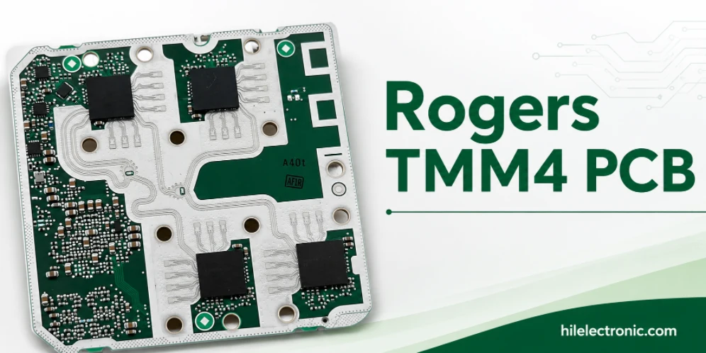
Rogers TMM4 PCB Manufacturer for Compact Microwave Filters
TMM4 is most useful when a microwave circuit must become...
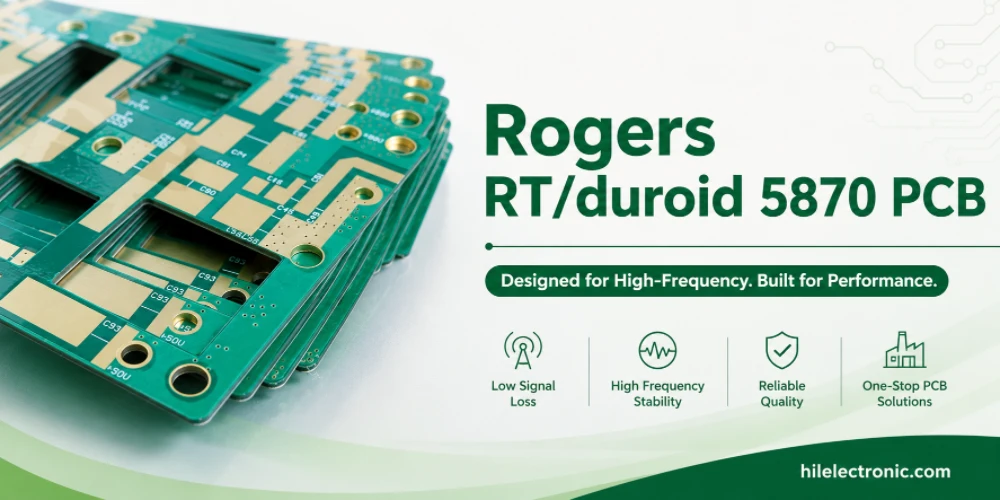
RT/duroid 5870 PCB Manufacturer for Low-Loss PTFE RF Circuits
RT/duroid 5870 is chosen when the RF path needs low loss,...
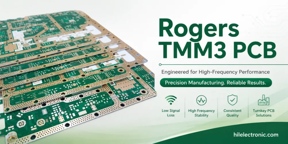
Rogers TMM3 PCB Manufacturer for Mechanical RF Modules
TMM3 is selected when an RF circuit must behave as part of...
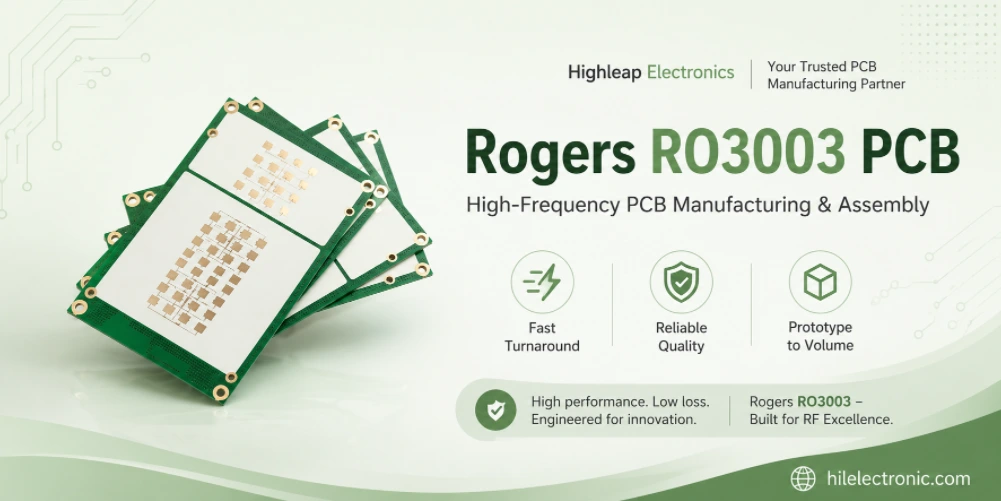
Rogers RO3003 PCB Manufacturer for Automotive Radar and mmWave Modules
A 77 GHz radar board is purchased as a working sensor...
How to get a quote for PCBs
Let‘s run DFM/DFA analysis for you and get back to you with a report. You can upload your files securely through our website. We require the following information in order to give you a quote:
-
- Gerber, ODB++, or .pcb, spec.
- BOM list if you require assembly
- Quantity
- Turn time
In addition to PCB manufacturing, we offer a comprehensive range of electronic services, including PCB design, PCBA, and turnkey solutions. Whether you need help with prototyping, design verification, component sourcing, or mass production, we provide end-to-end support to ensure your project’s success.
For PCBA services, please provide your BOM (Bill of Materials) and any specific assembly instructions. We also offer DFM/DFA analysis to optimize your designs for manufacturability and assembly, ensuring a smooth production process.