
Controlled-Depth Drilling PCB Manufacturing
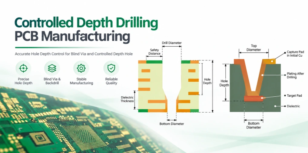
Yes—Highleap Electronics provides controlled-depth PCB drilling and backdrilling for advanced multilayer boards. We support high-speed PCB projects where plated via stubs must be removed to a specified depth without damaging the required interconnect. Our engineering team reviews the drill map, stack-up, residual-stub limits and inspection plan before confirming the manufacturing route.
For hardware designers, signal-integrity engineers and global OEM sourcing teams, the key question is not whether a supplier has a CNC drill. It is whether the supplier can preserve the target layer, control Z-axis depth and registration across production, and provide evidence that the released backdrill specification was met. Highleap combines PCB fabrication with optional component sourcing and PCB assembly for projects headed to prototype, NPI or volume supply.
Send the proposed layer stack, fabrication files, backdrill entry side and stop layer, primary/backdrill diameters, maximum residual-stub length and order quantity. We will assess the combined requirement; no single generic depth tolerance is suitable for every build.
The 60-layer figure describes Highleap's published overall rigid-PCB capability. Backdrill geometry, achievable stub length, tolerance, and available test methods are approved per design and must not be inferred from the layer-count limit.
Can Highleap Manufacture Controlled-Depth Drilled PCBs? Yes.
Highleap is a China-based PCB fabrication and assembly supplier with published services for PCB backdrilling, high-speed rigid boards and HDI manufacturing. For a typical controlled-depth backdrilling requirement, an already plated through-hole is re-entered with an appropriately larger tool. The unused plated copper barrel is removed to a controlled depth, while the necessary signal connection remains intact.
Our role is to review the entire build—not just accept a list of drill coordinates. The correct drilling depth depends on the released layer stack, the actual signal connection, the via barrel to be removed, the allowed residual stub and the position of the next protected copper layer.
Highleap's rigid PCB capability and high-frequency manufacturing services support projects such as high-speed network boards, server platforms, communication systems and dense multilayer instrumentation. Specific controlled-depth features remain subject to engineering approval.
Controlled-Depth Backdrilling: What Your SI Engineer Needs Preserved
In high-speed digital PCB design, controlled-depth drilling (CDD) is often another name for backdrilling. A plated through-hole that connects a signal between selected layers can leave an unused conductive section beyond that transition. This via stub may introduce a frequency-dependent resonance, reflections and channel discontinuities. Backdrilling removes most of that unused barrel without severing the intended signal path.
Stub removal is not an automatic requirement for every high-speed board. The decision should be tied to channel simulation, operating bandwidth, connector/via topology and the signal-integrity budget. A validated residual-stub requirement is more useful to a fabricator than a generic instruction such as “backdrill all high-speed vias.”
| Drawing / file input | Why the manufacturer needs it | Typical failure if ambiguous |
|---|---|---|
| Signal entry and exit layers | Identifies the required portion of the plated barrel | Backdrill cuts into the intended electrical connection |
| Drill origin: top or bottom | Sets the machining side and depth group | Unwanted stub remains, or the wrong barrel section is removed |
| Stop layer / target depth and datum | Defines the Z-axis endpoint against the approved stack | Excessive depth or unintended copper exposure |
| Maximum remaining stub length | Turns SI analysis into a measurable acceptance limit | Signal path passes electrical continuity but fails channel performance |
| Primary and backdrill diameters | Ensures unwanted plating is removed with workable clearance | Plating remains or nearby annular copper is damaged |
| XY coordinates, drill groups and keep-outs | Controls registration, routing clearances and tooling | Drill-to-copper violations or cross-group mix-ups |
Example: On a 16-layer PCB, a signal may use a plated via connection between L1 and L6 while the plated barrel continues toward L16. An approved backdrill from the opposite surface can remove most of the unused barrel beneath L6, leaving a specified residual stub. The stop point, tool size and entry side must follow the actual approved stack-up; this example is not a universal machine setting.
Six Process Controls We Discuss Before a Backdrilled PCB Is Released
Qualified buyers need a repeatable process, not an isolated claim about drilling accuracy. The manufacturing decision is shaped by the combination of material, stack-up, hole geometry and inspection requirement.
01 · Stack-up and Z-axis reference
Backdrill depth must relate to the released laminate build and a defined surface or layer datum. Finished thickness tolerance, dielectric variation, copper thickness and panel flatness can change the actual distance to the protected layer. Revisions to the stack-up require the drilling program and stub calculation to be reviewed again.
02 · Target-layer protection
The tool must remove unwanted barrel copper while maintaining a safe separation from the required connection. Specify protected layers, pads, antipads, nearby routes and acceptable remaining material. An aggressive stub requirement may not coexist with the available copper-to-drill clearance.
03 · Drill oversize and registration
A backdrill tool must be large enough to clear the plated barrel but not so large that it violates adjacent copper geometry. We review the relationship between primary drill, plating, backdrill diameter, annular rings and layer-to-layer registration. Critical BGA and connector fields deserve additional attention.
04 · Multi-depth and double-sided drilling
A board may require several stop layers or drilling from both surfaces. Every drill group needs unambiguous coordinates, side, target, diameter and stop condition. The groups should be distinguished in NC drill data and fabrication notes rather than hidden behind a single “CDD required” note.
05 · High-speed materials and hole quality
Low-loss laminates, glass styles, copper foil and board thickness can affect machining and inspection. Material alternatives should be approved by electrical engineering before release. Backdrilling must also be compatible with the preceding plated-hole and subsequent cleaning and finishing process.
06 · Acceptance plan and traceability
The order should define whether residual-stub verification uses first-article or production coupons, cross-sections, dimensional inspection or other agreed checks. Electrical continuity testing cannot by itself demonstrate that an unwanted conductive stub has been removed to the specified length.
For complex designs, the DFM discussion should involve fabrication engineering and the customer's signal-integrity team. This is especially important where a backdrill target competes with layer registration or mechanical thickness tolerance.
How We Approach Verification of Controlled-Depth Drilled Features
For a mission-critical PCB, “controlled depth” must be translated into measurable acceptance criteria. A suitable plan can include inspection of the drilled geometry and the location of the remaining barrel relative to the required copper layer, with sample frequency and reporting specified by the customer and agreed before production.
Evidence to request during supplier qualification
- Approved stack-up and backdrill layer-pair map
- First-article / coupon microsection showing the remaining stub and target-layer clearance
- Specified sampling plan and report format
- Hole quality, plating and electrical test requirements for the complete board
- Impedance or channel verification, if included in the agreed acceptance scope
- Revision-controlled drawings, materials and inspection records
Microsection evidence is useful when the key risk is internal residual-stub geometry that cannot be seen from outside the board. Dimensional methods may support accessible controlled-depth features. TDR or S-parameter testing, if commissioned, evaluates electrical behavior, but should not be mislabeled as direct proof of physical drill depth.
Highleap publicly describes AOI, electrical testing and advanced multilayer inspection as part of its PCB operations. The exact method, sampling and report commitment for a controlled-depth program must be agreed for the specific RFQ, rather than assumed from a general factory capability page.
Backdrilling vs Blind Vias vs Controlled-Depth Milling
The search term “controlled-depth drilling” is sometimes applied broadly to several partial-depth operations. For engineering purchase orders, the process must follow the feature function, not only the keyword.
| Feature / technique | Primary function | What belongs in the RFQ |
|---|---|---|
| Backdrilling (CDD) | Remove an unused section of a previously plated through-hole barrel | Entry side, plated via coordinates, target layer, drill oversize, maximum stub |
| Mechanically drilled blind via | Create a plated electrical connection that stops at an intended layer | Start/stop layers, drill diameter, aspect ratio, plating and lamination sequence |
| Laser microvia / HDI | Create a fine interconnect between selected build-up layers | Laser via geometry, target pad, stacked/staggered construction, fill and reliability requirements |
| Depth-milled cavity / counterbore | Create a local recess for mechanical, thermal or component accommodation | 2D geometry, depth datum, remaining floor, wall/floor finish, copper keep-outs |
Highleap reviews HDI interconnect options as well as controlled-depth backdrilling. Mechanical pockets and countersinks should be quoted from a separate mechanical drawing and are not a substitute for the high-speed backdrill process. For more process background, see our PCB backdrilling explanation.
A China PCB Manufacturing Partner for European and Israeli OEMs
Highleap Electronics serves international PCB and PCBA projects. For professional sourcing teams in Israel, Germany, France, the UK, the Netherlands and other European markets, our value proposition is the combination of advanced PCB fabrication, engineering discussion and optional assembly—not simply a low board price.
- Technical review before production: evaluate the residual-stub requirement, target-layer safety margin, drill data and build complexity at the RFQ stage.
- China manufacturing scale: Highleap's published rigid-PCB range extends to 60 layers, with high-speed, multilayer and HDI services relevant to complex board programs.
- PCB fabrication and assembly: coordinate the bare board with component sourcing and PCBA where a complete electronics manufacturing solution is required.
- Supplier-qualification discipline: specify acceptance class, revision control, traceability, inspection records, material declarations and any customer audit requirements.
- Export and commercial planning: agree delivery destination, freight terms, import documentation, confidentiality requirements and program milestones before order release.
Highleap's public company profile lists management-system certifications, including ISO 9001, ISO 13485 and IATF 16949. Ask for current certificate copies and the relevant site/process scope during supplier approval; certificates do not by themselves establish that a particular backdrilled design meets its requirements.
How to Request a Controlled-Depth Drilling PCB Quote
For a credible quotation, supply the approved or proposed stack-up and distinguish which vias require stub removal. A Gerber archive plus the note “controlled depth drilling” is generally not sufficient to determine a safe depth-control process.
| RFQ input | Minimum useful detail |
|---|---|
| Fabrication data | Gerber / ODB++, NC drill files, layer order, drawing revision and PCB outline |
| Full stack-up | Layer numbers, copper weights, dielectric materials and thicknesses, finished board thickness |
| Backdrill map | Coordinate set or dedicated NC files, tool sizes, drilling side and separate depth groups |
| Backdrill targets | Signal-connected layers, protected layer, depth datum, maximum allowed residual stub |
| Geometry & clearances | Primary finished hole, planned backdrill diameter, pad/antipad and copper keep-outs |
| Acceptance plan | IPC class or customer specification, coupon/microsection scope, report and sampling requirements |
| Commercial scope | Prototype/pilot/volume quantity, preferred material, delivery date, destination and incoterm |
| If assembly is needed | BOM, placement files, assembly drawing, component sourcing and functional test requirements |
What Drives Cost and Lead Time?
Controlled-depth drilling adds engineering setup, a dedicated machining operation and potentially destructive inspection. The commercial impact depends on the number of backdrill hits, number of depth groups, one- or two-sided access, tool diameter, material, layer count, required residual stub, sample/report requirements and manufacturing quantity. A tight stub constraint can change feasibility and yield—not just price.
Do not accept a fixed lead-time or universal residual-stub claim without checking it against your approved stack-up. We recommend quoting prototype, pilot and production volumes with the same defined acceptance scope where possible.
From Your Data Package to a Released Build
- Send the filesProvide stack-up, NC data, drill groups, stub limit and quantity.
- DFM discussionConfirm depth datum, target-layer protection, drill size, inspection and materials.
- Approve scopeRelease the drawing revision, quote, lead time and acceptance requirements.
- Build & verifyFabricate and inspect according to the agreed package; arrange PCBA if included.
Controlled-Depth Drilling PCB Manufacturing: FAQs
Does Highleap offer controlled-depth drilling or PCB backdrilling?
Yes. Highleap publicly offers backdrilling and advanced high-speed PCB fabrication. Submit the layer stack, via drill map and required residual stub so engineering can approve the specific construction and depth-control requirement.
Are controlled-depth drilling and backdrilling the same process?
In high-speed PCB terminology, controlled-depth drilling often refers to backdrilling to remove unwanted plated via stubs. “Controlled depth” can also describe other partial-depth operations. The fabrication drawing should identify the intended feature, whether it is plated and the exact function.
What residual via-stub length can Highleap guarantee?
There is no universal value for every stack-up. Give us the maximum residual stub allowed by your SI design and the location of the protected layer. Highleap must confirm the achievable depth/tolerance and verification plan for that specific construction before order release.
Can you backdrill from both sides or to different layer depths?
Such requirements can be submitted for engineering review. Provide distinct drill groups, entry sides, target layers, diameters and coordinate files. Combined feasibility is subject to available material thickness and copper clearance.
Will ordinary electrical testing prove the stub was removed?
No. Continuity/isolation testing can establish certain electrical connections and shorts but does not directly measure the remaining copper stub. If the residual stub is critical, specify an appropriate coupon/microsection or other agreed geometric verification method.
Can Highleap also supply assembled high-speed PCBs?
Yes. Highleap offers PCB fabrication and assembly services. Include the BOM, placement data, assembly notes and testing requirements if you want a combined quotation.
Can a European or Israeli company order backdrilled PCBs from Highleap?
Highleap serves international PCB/PCBA projects. Provide the destination, target incoterm, quality documentation and any confidentiality requirements at RFQ stage; specific shipping and contractual arrangements are agreed for the order.

Recommended Posts
Embedded Passive PCB Manufacturing for Integrated Designs
Highleap Electronics provides embedded passive PCB...
Cavity PCB Manufacturing for Precision Board Designs
A cavity PCB is a purpose-built board with a recessed or...
VIPPO PCB Fabrication for BGA and Thermal Pad Designs
Highleap Electronics provides VIPPO PCB fabrication for...

High Reliability PCB Assembly: Process Control and Traceability
Highleap Electronics manufactures high reliability PCB...
How to get a quote for PCBs
Let‘s run DFM/DFA analysis for you and get back to you with a report. You can upload your files securely through our website. We require the following information in order to give you a quote:
-
- Gerber, ODB++, or .pcb, spec.
- BOM list if you require assembly
- Quantity
- Turn time
In addition to PCB manufacturing, we offer a comprehensive range of electronic services, including PCB design, PCBA, and turnkey solutions. Whether you need help with prototyping, design verification, component sourcing, or mass production, we provide end-to-end support to ensure your project’s success.
For PCBA services, please provide your BOM (Bill of Materials) and any specific assembly instructions. We also offer DFM/DFA analysis to optimize your designs for manufacturability and assembly, ensuring a smooth production process.