
FR4 Dielectric Constant Calculator and PCB Design Guide
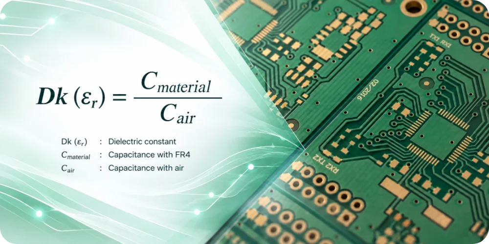
What is the dielectric constant of FR4? Most common FR4 laminates fall around Dk 4.0–4.5, but the correct value depends on material construction and frequency. Use the live calculator below to estimate signal delay, velocity, guided wavelength and preliminary microstrip impedance.
FR4 Dielectric Constant Calculator
Change any input. Results update immediately—no signup, page reload, or external service.
For your specified trace length
| Parameter | Material A | Material B |
|---|---|---|
| Bulk Dk | — | — |
| Effective Dk | — | — |
| Delay (ps) | — | — |
| Approx. Z₀ (Ω) | — | — |
What Is the Dielectric Constant of FR4?
The FR4 dielectric constant (Dk, or relative permittivity εr) is a measure of how the PCB's insulating laminate responds to an electric field. For preliminary designs, engineers often use Dk ≈ 4.0–4.5, but that is not a guaranteed value for all FR4. FR4 refers to a family of glass-reinforced epoxy materials with different resin systems, fabric constructions, and electrical characteristics.
The correct FR4 Dk depends on the specified laminate, glass style, resin content, operating frequency, and test method. A single “FR4 = 4.4” assumption is especially risky for controlled-impedance and high-speed layouts.
FR4 Dielectric Constant vs. Frequency: Real Manufacturer Data
FR4 exhibits dielectric dispersion: its Dk can change with frequency. The following Isola 370HR examples are construction-specific published figures—not universal values for every FR4 PCB.
| 370HR core construction | Resin content | Dk @ 100 MHz | Dk @ 1 GHz | Dk @ 10 GHz |
|---|---|---|---|---|
| 1×10⁶; 0.051 mm core | 71% | 3.89 | 3.81 | 3.63 |
| 1×1080; 0.064 mm core | 58% | 4.11 | 4.04 | 3.88 |
Source: Isola 370HR official construction-specific Dk/Df tables. Values are for the stated constructions and test conditions.
The table reveals two important facts: the same FR4 material family can have different Dk values because its construction differs, and a Dk measured at 1 GHz should not automatically be applied at 10 GHz. In the calculator, frequency is used for guided wavelength and phase; it does not invent a Dk-versus-frequency curve.
How the Calculator Works: The Actual Formulas
The calculator treats the signal path as an ideal, lossless, nonmagnetic transmission line. It first determines the effective relative permittivity and then calculates propagation velocity and delay:
v = c / √εeffDelay (ps) = Length (mm) × √εeff × 1000 / 299.792458Guided wavelength (mm) = v (mm/ns) / f (GHz)Electrical length (°) = 360 × Length / WavelengthHere, c = 299.792458 mm/ns. The effective relative permittivity (εeff) depends on the transmission-line cross-section:
Stripline: Fully Embedded Trace
For the ideal homogeneous stripline model, εeff = Dk. This makes the delay calculation particularly simple, but it does not calculate stripline impedance. Actual stripline impedance needs the trace dimensions, copper thickness, plane spacing, and stackup details.
Microstrip: Surface Trace
A microstrip trace has fields in both air and the PCB substrate. The calculator uses a common quasi-static approximation for εeff based on the trace width W, dielectric height h, and bulk Dk. The result is lower than bulk Dk for a conventional air-exposed microstrip.
For microstrip only, the tool also shows a preliminary characteristic impedance Z₀ using a zero-conductor-thickness closed-form approximation. This does not include solder mask, finite copper thickness, copper roughness, frequency dispersion, or manufacturing tolerances; it cannot replace your board shop's impedance field solver.
Worked Example: Dk 4.2 vs. 3.8
For an ideal embedded 50 mm transmission line, Dk = 4.2 produces approximately 341.80 ps of one-way delay, while Dk = 3.8 produces approximately 325.12 ps. That is a 16.68 ps difference over the same physical length. Change the line length or switch to Microstrip in the calculator above to see the corresponding results for your geometry.
FR4 Dk vs. Df: Why Both Matter
Dk influences electromagnetic propagation, phase velocity, and transmission-line impedance. Df (dissipation factor, or loss tangent) describes dielectric energy loss and contributes to signal attenuation. A PCB material with lower Dk does not automatically have lower Df or lower total insertion loss. High-speed and RF material selection must consider both, alongside copper loss, roughness, and circuit geometry.
How Dk Affects 50-Ohm and 100-Ohm PCB Routing
Dielectric properties affect the characteristic impedance of 50 Ω single-ended traces and 90/100 Ω differential pairs, but Dk alone is insufficient to calculate impedance. A reliable controlled-impedance calculation requires stackup geometry, reference-plane arrangement, finished copper thickness, line width, and—in differential pairs—trace spacing and coupling.
Use the microstrip Z₀ result above for early concept checks only. For final fabrication, provide Highleap Electronics with controlled-impedance targets and a proposed stackup so appropriate geometry and material assumptions can be reviewed.
What to Send a PCB Manufacturer
For an FR4 PCB with controlled impedance or demanding high-speed signals, include the laminate grade (or approved alternatives), layer stackup, core/prepreg details if available, finished copper requirements, controlled nets and target impedances, tolerances, fabrication files, and any loss or timing constraints. For complete PCB assembly projects, also provide the BOM, component placement data, and assembly requirements.
Highleap Electronics offers PCB fabrication and PCB assembly services. A manufacturable stackup should consider material availability, dielectric thickness, fabrication tolerances, assembly heating, and long-term reliability—not just a nominal Dk number.
FR4 Dielectric Constant: Frequently Asked Questions
What is the dielectric constant of FR4?
Many commonly used FR4 laminates are roughly in the 4.0–4.5 range, but there is no single universal value. Use the actual material's documented Dk at a relevant frequency for final design calculations.
What is the FR4 dielectric constant at 1 GHz?
It depends on the laminate construction. For example, Isola 370HR 1×1080 core with 58% resin has a published Dk of 4.04 at 1 GHz; other constructions differ.
What is the FR4 dielectric constant at 10 GHz?
It depends on the product and construction. Isola 370HR's 1×1080, 58% resin core is published at Dk = 3.88 at 10 GHz. Do not apply this value to another FR4 grade without verification.
Can I calculate 50-ohm trace width using Dk alone?
No. The required trace width also depends on dielectric height, conductor thickness, trace geometry, and other stackup details. Our microstrip impedance result is a preliminary zero-thickness approximation, not a production sign-off.
Why are stripline and microstrip delays different?
An ideal embedded stripline's fields are in the substrate, so εeff approximately equals material Dk. An air-exposed microstrip shares its fields between substrate and air, giving a lower εeff and generally faster propagation for the same bulk Dk.
Does choosing a higher frequency automatically lower Dk?
Not in a reliable, universal way. Dk has material-specific frequency dispersion. This tool never changes your Dk input when frequency changes; you should enter a supplier-published value or a validated frequency-dependent model.
Need a Controlled-Impedance FR4 PCB?
Send Highleap Electronics your stackup, fabrication files, impedance targets, and assembly requirements. We can discuss your PCB manufacturing and PCBA needs with the actual design constraints in view.
Contact Highleap Electronics →
Recommended Posts
TMM13i PCB Manufacturing
TMM13i PCB manufacturing is aimed at ultra-compact RF...

TMM10 PCB Manufacturing for Compact RF Designs
Table of contentsHow TMM10 Shrinks RF StructuresTMM10 vs...
TMM Temperature Stable PCB Manufacturing
Table of Contents Rogers TMM Temperature Stable PCB...

TMM PCB for Antenna Miniaturization
The antenna-miniaturization page is intentionally narrower...
How to get a quote for PCBs
Let’s run DFM/DFA analysis for you and get back to you with a report. You can upload your files securely through our website. We require the following information in order to give you a quote:
-
- Gerber, ODB++, or .pcb, spec.
- BOM list if you require assembly
- Quantity
- Turn time
For PCBA services, please provide your BOM (Bill of Materials) and any specific assembly instructions. We also offer DFM/DFA analysis to optimize your designs for manufacturability and assembly, ensuring a smooth production process.