
Gerber Viewer: How to Check PCB Files Before Fabrication

Figure 1. Gerber viewer for PCB file checking
Last updated: May 2026 · A practical guide to viewing and verifying Gerber data
A Gerber viewer is a tool that renders the Gerber and drill files exported by your PCB software so you can see exactly what the fabricator will build. Opening your output in an independent viewer before you place an order is the single most valuable habit in PCB design — it catches missing layers, swapped masks, wrong drill sizes, and silkscreen sitting on pads while a fix still costs nothing. This guide explains what Gerber files are, walks through the best free online and desktop viewers (including Highleap’s own online viewer), and shows what to look for layer by layer.
What Is a Gerber File? (And What a Gerber Viewer Shows)
Gerber is the de facto standard image format for PCB fabrication. Each Gerber file describes one layer of the board as 2D artwork — copper, solder mask, silkscreen, paste — using draw commands and an aperture list. A complete board is a set of these files (top copper, bottom copper, top/bottom mask, top/bottom silk, and so on), accompanied by an Excellon drill file that lists every hole’s size and position, plus a board outline. The modern revision, Gerber X2 (RS-274X2), embeds extra attributes — which layer is which, what each pad is for — so viewers and fabricators can interpret the data without guesswork.
Why You Should Always View Gerber Files Before Ordering
Designers regularly discover problems only when they open the exported files in a viewer, not in their editor. Common catches include:
- A layer that didn’t export, or two layers swapped.
- Solder mask missing over pads, or mask covering pads that should be open.
- Silkscreen text overlapping pads or hanging off the board edge.
- Drill hits that don’t line up with their copper pads (a drill/copper registration error).
- A board outline on the wrong layer, so the fab can’t find the shape.
None of these are visible from inside your design tool’s normal view. Five minutes in a viewer prevents a wasted order and a lost week.
Best Free Online Gerber Viewers
Browser-based viewers need no install and are ideal for a quick pre-order check or for sharing a board with someone who has no EDA software.
Highleap online Gerber Viewer
Highleap provides a free online Gerber viewer directly on the site — upload your file set and inspect the rendered layers in the browser. Because it sits next to the quoting workflow, it’s a convenient way to confirm your data looks right before requesting fabrication. There’s also a companion 3D viewer for visualising the assembled board.
Altium 365 Viewer
Altium’s free, browser-based Altium 365 Viewer opens Gerber (RS-274X and X2) as well as native Altium, EAGLE, KiCad (beta), and ODB++ data. It offers schematic/PCB/3D views, cross-probing, layer-stack inspection, and point-to-point measurement, with optional shareable links. Uploaded designs are removed when you close the browser session unless you choose to save or share them.
Manufacturer web viewers
Many fabricators embed an online viewer in their order flow so you can preview the board you’re about to buy. They’re handy for a final sanity check, though they vary in how much detail they expose.
Best Desktop Gerber Viewers (Free and Offline)
Desktop viewers give you finer control, work offline, and suit repeated use during a design.
| Tool | Cost / platform | Notes |
|---|---|---|
| KiCad GerbView | Free, open source; Win/macOS/Linux | Bundled with KiCad; reads Gerber + Excellon; excellent layer control |
| gerbv | Free, open source; Win/Linux | Lightweight gEDA viewer; loads multiple layers with colour and transparency |
| ViewMate (Pentalogix) | Free viewer; Windows | Long-established Gerber viewer/editor; measurement and inspection tools |
| ZofzPCB | Free; Windows | 3D Gerber viewer — see the board built up layer by layer |
If you already use KiCad, its built-in GerbView is the easiest choice; for a standalone Windows reader, ViewMate is the classic; for a 3D look at the stack, ZofzPCB is hard to beat.
What to Check in a Gerber Viewer, Layer by Layer
Open every layer and step through this list:
- Copper (top/bottom): traces, pours, and pads are present and unbroken; copper-to-edge clearance is sane.
- Solder mask: openings sit exactly over pads, not over traces; no mask covering a pad you need to solder.
- Silkscreen: reference designators are readable and clear of pads and the board edge.
- Drill: every hole lines up with a pad; pad and via sizes match what you intended.
- Paste (if assembling): stencil apertures match the pads they belong to.
- Outline: the board profile is a single closed shape on the correct layer.
- Layer count and order: the right number of copper layers, named correctly.
How to View Gerber Files: Step by Step
- Export a complete Gerber set plus the NC drill file from your EDA tool; most exports produce a folder or a ZIP.
- Open the viewer — drag the whole folder or ZIP into an online viewer, or open the files in a desktop tool.
- Toggle layers on and off and switch colours so you can read each one clearly.
- Overlay copper and drill to confirm holes register with pads.
- Measure a known feature (a connector pitch, the board width) to confirm scale and units are correct.
- Fix and re-export if anything is off, then view again — never order until the viewer matches your intent.
Gerber, X2, Excellon, and ODB++ File Formats Explained
A few formats travel together. RS-274X is the long-standing extended Gerber; X2 adds machine-readable attributes and is preferred today. The Excellon file carries drill data. ODB++ (and IPC-2581) is an alternative that bundles copper, drill, netlist, and component data into one consistent package, reducing the risk of mismatched files. A good viewer reads Gerber and Excellon at minimum; many also read ODB++.
Common Gerber File Problems and How to Spot Them
A viewer is most useful when you know what each defect looks like on screen. The table below maps the symptom you’ll see to its likely cause and the fix — the mental checklist that turns a quick preview into a real inspection.
| What you see in the viewer | Likely cause | Fix |
|---|---|---|
| Pads look bare copper with no green/coloured ring around them | Solder-mask layer didn’t export, or mask openings are missing | Re-export the mask layers; confirm mask-opening rules in the footprint |
| Pads are covered and don’t show an opening | Mask is over the pad (tented) when it should be open | Adjust solder-mask expansion so the pad is exposed |
| Holes sit off-centre from their pads | Drill/copper registration mismatch or wrong drill file | Re-export the NC drill aligned to the same origin as the copper |
| Text sits on top of pads or runs off the edge | Silkscreen not clipped to mask/board outline | Move or shrink reference designators; enable silk clipping |
| A copper layer is blank or duplicated | A layer failed to export, or two were mapped to the same file | Re-check the layer-to-file mapping in the export dialog |
| The board has no visible outline | Outline drawn on a non-exported mechanical layer | Place the outline on the layer the fab expects and re-export |
| Everything looks tiny or huge when measured | Unit or format mismatch (inch vs mm, leading/trailing zeros) | Set the viewer to the file’s units; re-export with explicit format |
Online vs Desktop Gerber Viewer: Which Should You Use?
Both kinds of viewer render the same data; they differ in convenience, privacy, and how often you’ll use them. Pick by situation rather than treating one as universally better.
| Consideration | Online viewer | Desktop viewer |
|---|---|---|
| Setup | None — open a browser and upload | Install once, then run offline |
| Best for | A quick pre-order check; sharing a board with someone without EDA tools | Repeated checks during a design; detailed layer work |
| Privacy | Files are uploaded to a server; check the retention policy for sensitive designs | Files never leave your machine |
| Depth of tools | Good for visual review and measurement | Finer control, scripting, and layer manipulation |
| Tie-in to ordering | A fab’s own viewer sits right next to the quote | Separate from any ordering flow |
A practical workflow uses both: a desktop viewer such as GerbView or gerbv during the design, then a manufacturer’s online viewer as the final check at the moment you order.
Free Gerber Viewer and DFM Check with Highleap
Highleap Electronics pairs a free online Gerber viewer and 3D viewer with a manufacturing workflow, so checking your data and ordering the board happen in one place:
- Preview first: upload and inspect your Gerber set in the browser before committing.
- DFM review: our engineers run a deeper check that catches the manufacturability issues a viewer alone won’t flag.
- Fabrication: from prototype to production, built from your verified Gerber or ODB++ data.
- Format flexibility: we accept Gerber (RS-274X/X2), Excellon drill, and ODB++.
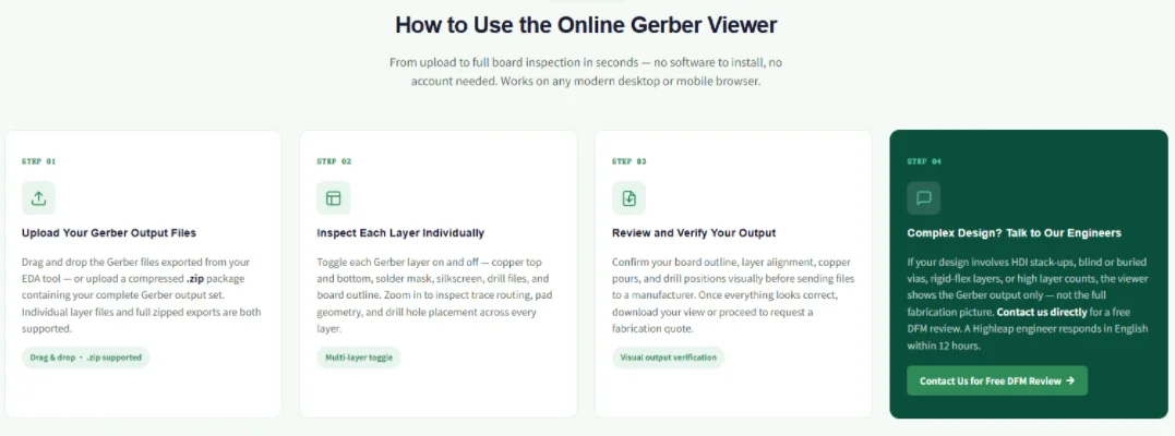
Figure 2. Gerber viewer for PCB file checking details
Gerber Viewer FAQ
What is a Gerber viewer used for?
To render your exported PCB layers as the fabricator will see them, so you can verify copper, mask, silkscreen, and drill data before ordering.
Is there a free online Gerber viewer?
Yes — Highleap’s online Gerber viewer and the free Altium 365 Viewer both run in a browser with no install, and KiCad’s GerbView is a free desktop option.
What is ViewMate?
ViewMate is a long-established free Gerber viewer for Windows from Pentalogix, with measurement and inspection tools. It’s a common standalone choice for reviewing Gerber data.
Can a Gerber viewer open drill files?
Most can. Load the Excellon drill file alongside the copper layers and overlay them to confirm every hole registers with its pad.
Do I still need a Gerber viewer if I use ODB++?
It’s still worth viewing. ODB++ reduces file-mismatch errors, but a visual check of every layer remains the best way to confirm the board matches your intent.
Will viewing my Gerbers catch every manufacturing problem?
No. A viewer catches data and artwork errors; it doesn’t judge manufacturability against a specific fab’s capabilities. Pair the visual check with a DFM review for full coverage.

Recommended Posts
TMM PCB Fabrication
Table of Contents TMM PCB Fabrication Scope for RF and...

RT duroid 6002 PCB Quote and Stackup
This page owns the quotation and stackup-definition task...
TMM6 Filter PCB Manufacturing
Table of contentsWhy Microwave Filter Designers Use...
Taconic RF 35 vs RO4350B PCB
Table of contentsRF-35 vs RO4350B Procurement and...
How to get a quote for PCBs
Let‘s run DFM/DFA analysis for you and get back to you with a report. You can upload your files securely through our website. We require the following information in order to give you a quote:
-
- Gerber, ODB++, or .pcb, spec.
- BOM list if you require assembly
- Quantity
- Turn time
For PCBA services, please provide your BOM (Bill of Materials) and any specific assembly instructions. We also offer DFM/DFA analysis to optimize your designs for manufacturability and assembly, ensuring a smooth production process.