
Stacked Microvia PCB Manufacturing
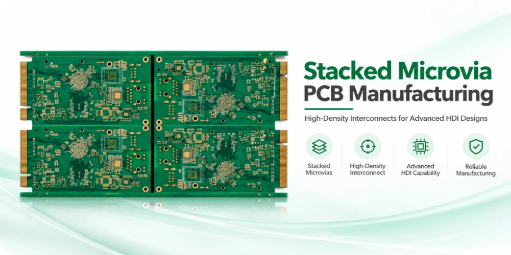
Highleap manufactures HDI PCBs with stacked microvia structures in China. Our capability includes laser-drilled microvias, copper-filled interconnects, sequential build-up and related multilayer PCB fabrication. The real qualification question is whether the complete via chain—not just an individual microvia—has the geometry, copper interfaces and evidence required by your product.
We work with OEM design and procurement teams on fine-pitch BGA escape, space-constrained HDI interconnects and production transfer. Bring us a proposed stack-up, even if it is not yet frozen: we can discuss whether a vertically stacked construction is necessary, where a staggered arrangement is viable, and which reliability checks belong in the manufacturing specification.
Already have the layer stack and microvia map? Send your HDI design for an engineering quotation.
The First Decision Is Whether the Vias Need to Be Stacked
A stacked microvia is an architectural choice with manufacturing consequences. It should solve a demonstrable routing or interconnect-density constraint, rather than appear as a default feature on every HDI board.
Successive laser microvias occupy substantially the same X-Y position across build-up dielectric layers. Each new level lands on the underlying connection, typically requiring a prepared, copper-filled and capped structure capable of supporting the next microvia. This arrangement can preserve routing channels beneath fine-pitch devices. It also creates additional copper-to-copper interfaces that deserve attention during process qualification.
Highleap's engineering discussion starts with the fan-out and layer connectivity: component pitch, pad field, trace/space constraints, reference planes, dielectric thickness, copper weights and the permitted via locations. If changing the arrangement alters return paths or impedance, that trade-off belongs to the customer's electrical design review.
See our related HDI PCB manufacturing and HDI stack-up design resources for broader construction choices. This page focuses specifically on making stacked microvia chains producible and supportable through qualification.
The Hard Part Is the Hidden Copper Interface
Stacked microvias are often presented as a straightforward route to denser wiring. For long-life and high-performance products, the more important issue is the integrity of the interface between the copper fill of one level and the target pad or cap supporting the next. Local voiding, incomplete fill, poor metallurgical bonding, contamination or processing variation can create a latent interconnect weakness.
This is not a theoretical objection to all stacked microvias. It is a known qualification issue. In 2019, IPC publicly warned that certain microvia failures were detected only after bare-board acceptance—during reflow, assembly stress screening or field use—and highlighted the risk of weak target-pad-to-copper-fill interfaces. It also cautioned that conventional microsection inspection alone may not catch every latent defect.
What this means for a manufacturing purchase order: specify performance-based acceptance and construction-representative testing where product risk warrants it. A beautiful cross-section photograph and a passing room-temperature continuity test are useful data points, but neither should be treated as complete proof of long-term stacked-microvia reliability.
Industry reference: IPC's microvia reliability warning, March 2019, and the referenced IPC-WP-023 white paper.
Target-pad interface
Weak adhesion or a compromised copper interface can open under thermal expansion. Define a test approach that is sensitive to the intended stacked-chain failure mode.
Fill quality
Voids, seams, excessive dimpling or incomplete copper fill may affect the next laser-drilled level. Confirm the intended copper-fill and cap construction before CAM release.
Registration and geometry
Dielectric thickness, laser taper, target-pad dimensions and registration margin interact. A nominal via diameter alone does not describe the production window.
For high-reliability programs, discuss via-chain coupons, reflow exposure, resistance monitoring during relevant thermal stress, microsection criteria and customer-specific acceptance requirements. Use the applicable revision of your contractual IPC or OEM specification. Neither the IPC warning nor a single test result makes every stacked construction unsafe—or every tested construction universally qualified.
How Highleap Evaluates a Production Stack
Stacked microvia PCB manufacturing is a repeated build-up process. Its cost and technical difficulty come from making each level ready to support the next—not simply from running a smaller drill. The exact process route depends on the laminate system and qualified factory method; the following is the sequence we align with customers at engineering review.
- Freeze the core and layer-pair definitionDocument the core, every build-up dielectric, copper weights, finished thickness, buried interconnects and stack locations. Assign an unambiguous layer number to each microvia start and target.
- Laminate and expose the intended target copperBuild the next dielectric layer; laser drill to the target pad under qualified registration and depth conditions. The target-pad preparation influences subsequent interfacial quality.
- Metallize, fill and prepare the landing surfaceSpecify electroplated copper fill and cap where the next microvia must land directly above. Control plating quality, voiding, planarity and subsequent copper surface preparation.
- Repeat only the approved stacked levelsEach additional build-up cycle adds handling, lamination exposure and an interface to control. Changes in stack height or a switch to staggered vias should be treated as a design revision.
- Inspect the chain, then plan assembly exposureReview the released fabrication criteria and qualification evidence. When via-in-pad sits beneath a BGA, align the finished surface and reflow exposure with the PCBA team.
What we want to see in a design package
A proper via table includes L1–L2, L2–L3 and any other levels separately; a drill symbol that says only “stacked via” leaves too much open to interpretation. Indicate whether the chain lands on a buried via, a through-hole pad or another copper feature. Include capture-pad dimensions, dielectric thickness, stack height, fill/cap requirements and via-in-pad status.
Highleap's published services include laser-drilled HDI, blind/buried vias, sequential lamination and copper-filled stacked structures. We confirm which combination is feasible for the customer's actual layer arrangement, material and volume; we do not publish one universal production recipe for every stacked stack-up.
Qualifying a Stacked-Microvia Supplier: Ask for Evidence, Not Adjectives
An HDI supplier's maximum layer count does not tell you whether its copper-filled stacked-via process matches your construction. For procurement managers and OEM quality teams, useful evidence is specific to the actual via chain, laminate and test exposure.
| Qualification question | Evidence to agree with the manufacturer |
|---|---|
| Is the exact stack height manufacturable? | Approved build-up drawing, via layer-pair map and the reviewed lamination sequence |
| How is the copper interface controlled? | Specified copper-fill/cap structure, target preparation and cross-sectional acceptance criteria |
| Does a representative sample survive assembly exposure? | Reflow/thermal test conditions, representative coupons, resistance monitoring where specified, pass/fail limits |
| How will the factory prevent revision drift? | Controlled stack-up, material list, drilling data, ECO approval and production record requirements |
| Can the first pilot lot support volume release? | First-article results, agreed test reports, nonconformance process and volume transition criteria |
We recommend locking the acceptance objective at RFQ stage. A sample microsection confirms conditions at that sample location; it is not interchangeable with performance-based reliability testing. Likewise, an electrical test at room temperature may miss a weakness that appears under thermal stress. The suitable combination depends on application risk and customer specification.
Highleap can coordinate advanced PCB fabrication with PCB assembly and component sourcing when the same program requires SMT, BGA placement, inspection and functional testing. Early fabrication/assembly coordination matters especially when stacked via-in-pad structures sit within fine-pitch BGA footprints.
From a Proposed HDI Stack-Up to a Meaningful Quote
A stacked-microvia quote should account for how the board will actually be made: number of build-up cycles, copper-filled levels, buried-via relationships, material system, panel yield, inspection and reliability qualification. Two boards of the same outline and layer count can have very different process routes and risk.
We work with international engineering and sourcing teams, including European and Israeli OEM programs, that need an accountable China PCB manufacturing partner. For these teams, supplier approval often involves engineering documentation, production traceability, materials and RoHS/REACH documentation where applicable, confidentiality terms, and agreement on shipping and inspection scope. Those details should be settled alongside the technical quotation, not after prototype approval.
Send these four groups of information
- Construction: Gerber or ODB++ package, full stack-up, dielectric/copper callouts and fabrication drawing.
- Via chain: drill files, microvia layer pairs, stack height, capture pads, fill/cap requirements, buried-via junctions and surface finish.
- Acceptance: intended IPC/customer class, microsection or via-chain coupon requirements, assembly reflow profile and any qualification plan.
- Commercial: prototype/pilot/volume quantities, required schedule, destination, approved material alternatives and whether PCBA is included.
If the stack-up is preliminary, label your non-negotiable electrical, mechanical and reliability constraints. Our engineering feedback can help identify whether the original stacked arrangement should be retained or redesigned before final routing.
Have a stacked-microvia design ready for review?
Send your actual layer build and we will discuss the manufacturable construction and RFQ scope.
Why Highleap for a Stacked Microvia PCB Program?
Highleap Electronics is a China-based PCB and PCBA manufacturing partner, with publicly described HDI laser drilling, copper-filled stacked via processes, multilayer lamination and integrated electronics assembly options. We are a fit for teams that want to discuss routing-density decisions and manufacturing risk with an engineering supplier—not purchase a generic board specified only by layer count.
The objective is a design that can progress from engineering evaluation to an approved, repeatable production build. That requires agreement on the actual stacked geometry, suitable material and process sequence, and reliability evidence proportional to product risk. Share your stack-up and request a manufacturing discussion with Highleap.

Recommended Posts
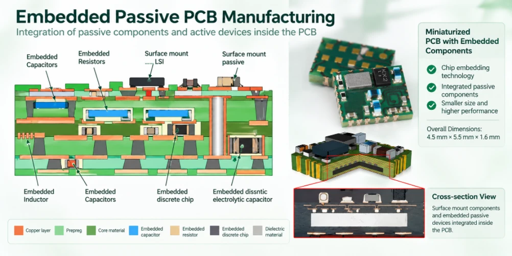
Embedded Passive PCB Manufacturing for Integrated Designs
Highleap Electronics provides embedded passive PCB...
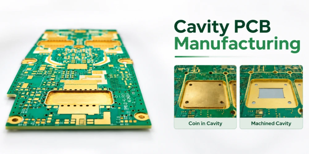
Cavity PCB Manufacturing for Precision Board Designs
A cavity PCB is a purpose-built board with a recessed or...
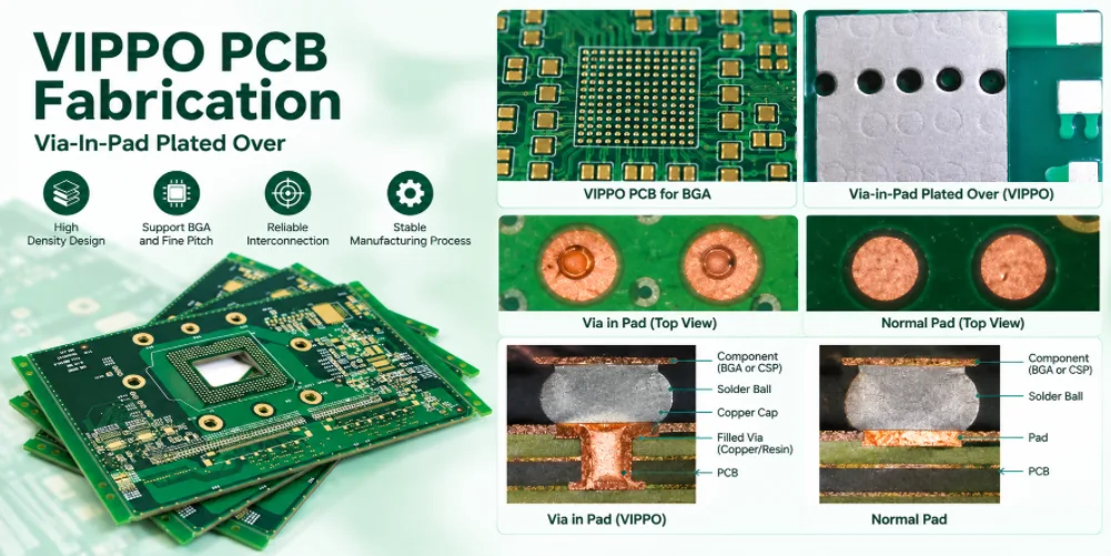
VIPPO PCB Fabrication for BGA and Thermal Pad Designs
Highleap Electronics provides VIPPO PCB fabrication for...

High Reliability PCB Assembly: Process Control and Traceability
Highleap Electronics manufactures high reliability PCB...
How to get a quote for PCBs
Let‘s run DFM/DFA analysis for you and get back to you with a report. You can upload your files securely through our website. We require the following information in order to give you a quote:
-
- Gerber, ODB++, or .pcb, spec.
- BOM list if you require assembly
- Quantity
- Turn time
In addition to PCB manufacturing, we offer a comprehensive range of electronic services, including PCB design, PCBA, and turnkey solutions. Whether you need help with prototyping, design verification, component sourcing, or mass production, we provide end-to-end support to ensure your project’s success.
For PCBA services, please provide your BOM (Bill of Materials) and any specific assembly instructions. We also offer DFM/DFA analysis to optimize your designs for manufacturability and assembly, ensuring a smooth production process.