
Capacitance Formula in PCB Design

Capacitance affects energy storage, filtering, timing, coupling, and power integrity throughout an electronic product. In PCB design, the basic formula is only the starting point: real behavior also depends on voltage bias, tolerance, ESR, ESL, placement, and the impedance created by the layout.
This article connects the capacitance formula to practical decisions in component selection and PCB assembly.
Table of contents
- The Capacitance Formula
- Real Capacitor Behavior
- Decoupling and Power Integrity
- PCB Parasitic Capacitance
- Component Selection and Assembly
- Design Review With Highleap Electronics
The Capacitance Formula
Capacitance is defined as C = Q / V, where C is capacitance, Q is stored charge, and V is voltage. For an ideal parallel-plate structure, capacitance is approximated by C = epsilon A / d: permittivity multiplied by plate area and divided by the separation distance.
These relationships explain why dielectric properties, conductor geometry, and spacing matter in both components and PCB structures. They do not, by themselves, predict the high-frequency behavior of a mounted capacitor.

Real Capacitor Behavior
A real capacitor includes parasitic resistance and inductance. As frequency increases, those parasitics can dominate and create a self-resonant point above which the part no longer behaves as an ideal capacitive element.
Review the component data for capacitance tolerance, DC-bias behavior, temperature characteristics, ESR, and impedance curves. This is especially important when MLCCs are used close to their rated voltage or in wide-temperature applications.

Decoupling and Power Integrity
Decoupling capacitors supply short bursts of current near an IC and reduce voltage movement on the power rail. Their effectiveness is strongly affected by the loop formed by the capacitor, power pin, ground return, and vias.
- Place the smallest high-frequency decouplers close to the relevant power pins.
- Use short, wide connections and a continuous reference plane where possible.
- Select capacitance values from the IC guidance and the measured or simulated power-demand profile.

PCB Parasitic Capacitance
Adjacent copper features also form capacitance. Plane pairs, traces over reference planes, pads, and connector structures can influence signal edges, coupling, and impedance. In controlled-impedance designs, stack-up data and field-solver calculations are more dependable than rules of thumb.
Keep sensitive nets separated from noisy switching nodes, and preserve a clear return path so that unavoidable parasitics do not create unexpected noise coupling.
Component Selection and Assembly
Select capacitor packages and dielectric types from the operating voltage, frequency range, temperature, required stability, and assembly constraints. Very small packages reduce mounting inductance but can be more sensitive to flex cracking if the board or depaneling process is not controlled.
Land patterns, solder paste apertures, reflow profile, and board support should be reviewed together for reliable assembly.
Design Review With Highleap Electronics
Highleap Electronics can review capacitor land patterns, placement constraints, stack-up information, and assembly requirements before production. Providing the critical power rails and any impedance requirements makes the review more focused.
For a manufacturability review, request a PCB quote with the Gerber files, BOM, and relevant design notes.
Get a Free PCB & PCBA Quote

Recommended Posts
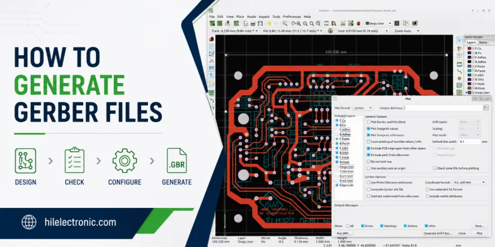
How to Generate Gerber Files for PCB Manufacturing
Figure 1. how to generate Gerber files image for Highleap...
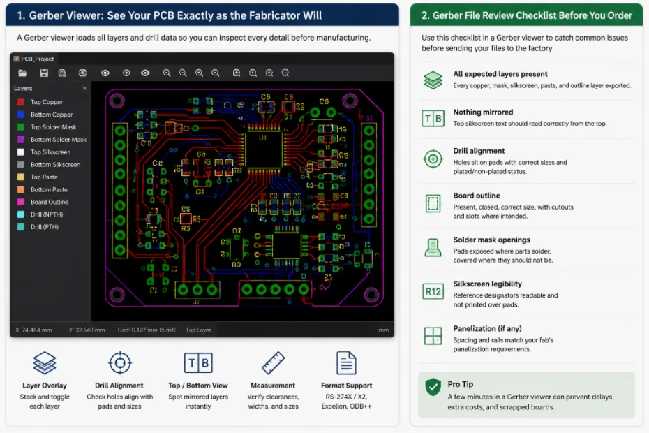
Gerber File Review Checklist: How to Check PCB Files Before You Order
Figure 1. Gerber file review catches missing layers, drill...
PCB Test Point Design Rules for Debug and ICT
Figure 1. PCB test point design rules help make debugging,...
PCB Jumper Wire: Uses, Types, and Design Tips
Figure 1. PCB jumper wires are useful for prototypes and...
How to get a quote for PCBs
Let us run DFM/DFA analysis for you and get back to you with a report.
You can upload your files securely through our website.
We require the following information in order to give you a quote:
-
- Gerber, ODB++, or .pcb, spec.
- BOM list if you require assembly
- Quantity
- Turn time
In addition to PCB manufacturing, we offer a comprehensive range of electronic services, including PCB design, PCBA (Printed Circuit Board Assembly), and turnkey solutions. Whether you need help with prototyping, design verification, component sourcing, or mass production, we provide end-to-end support to ensure your project’s success. For PCBA services, please provide your BOM (Bill of Materials) and any specific assembly instructions. We also offer DFM/DFA analysis to optimize your designs for manufacturability and assembly, ensuring a smooth production process.