
How PCB Coils Enhance Circuit Efficiency and Performance

A PCB coil, also known as an integrated PCB inductor, is a type of inductor created directly on a printed circuit board (PCB) using the copper traces. These coils play a vital role in various electronic circuits by generating a magnetic field when current flows through them, providing inductance for energy storage and signal processing. The integration of PCB coils into the PCB itself allows for a more efficient and compact solution compared to traditional discrete inductors. This article explores the design principles, fabrication methods, performance parameters, applications, and advantages of PCB coils over discrete inductive components.
What is a PCB Coil?
A PCB coil is a custom inductor designed using the copper traces on a PCB to create a coiled structure. The coil can take several forms, including spirals, serpentine patterns, or more complex helical configurations, depending on the required inductance and application. When an electric current passes through the coil, it generates a magnetic field, which stores energy momentarily and resists changes in current. This characteristic makes PCB coils essential for many applications, such as power supplies, signal processing, and energy storage systems.
By embedding the inductor directly into the PCB, engineers eliminate the need for discrete inductive components, leading to cost savings, reduced space usage, and simplified assembly processes. The inductance value of a PCB coil is determined by several factors, including the number of turns, the trace width, and the spacing between turns.
Types of PCB Coils
PCB coils come in several configurations, each designed to meet different application needs. The most common types of PCB coils include spiral, serpentine, helical, and toroidal coils. These types offer unique benefits based on factors like inductance, footprint, and performance under specific operational conditions.
Spiral Coils
Spiral coils are formed by winding copper traces in a spiral pattern, either clockwise or counterclockwise. This type of coil offers a compact design with a high inductance density, making it ideal for applications where space is limited. Due to their simplicity, spiral coils are widely used in power supplies and RF circuits, where space constraints and efficient energy storage are key priorities.
Serpentine Coils
Serpentine coils are designed with copper traces that wind back and forth in a zigzag or snake-like pattern. This type is simpler to layout compared to spiral coils and is ideal for achieving higher inductance values in a limited space. However, serpentine coils can be limited by their frequency response. These coils are commonly used in low-frequency power filters and other circuits where minimizing space and cost is essential.
Helical Coils
Helical coils are three-dimensional coils formed by extending copper traces across multiple PCB layers using plated through-hole vias. This design allows for higher inductance values and better current handling capabilities, making it suitable for high-performance applications. These coils are typically found in high-power systems, including power converters and high-frequency RF circuits, where greater inductive properties are required.
Toroidal Coils
Toroidal coils feature a closed-loop, donut-shaped design with copper traces wound around a circular core. This configuration offers stable inductance and an excellent Q-factor (quality factor), which helps reduce losses and improves energy efficiency. Toroidal coils are commonly used in precision power supplies, RF amplifiers, and EMI filters, where maintaining consistent performance and minimizing interference is crucial.
The choice of PCB coil type depends on the specific application requirements, such as inductance, frequency range, space, and current handling. Spiral and serpentine coils are ideal for compact, cost-effective solutions, while helical and toroidal coils are better suited for high-performance, high-power applications. Each coil type has its unique advantages, and selecting the right one can significantly enhance the efficiency and reliability of the overall electronic system. Whether used in power supplies, RF circuits, or filtering applications, PCB coils provide a versatile and efficient solution for integrating inductance into modern electronic designs.

How Do PCB Coils Work?
PCB coils operate on the same fundamental electromagnetic principles as traditional wire-wound inductors. The current flowing through the copper traces generates a magnetic field around the coil. The core principle behind this behavior is inductance, which resists changes in current and stores energy within the magnetic field. The magnetic field generated by the coil increases with the number of turns, and the inductance is affected by the trace width, spacing, and current frequency.
- Inductance: The ability of the coil to resist changes in current flow. This is determined by the coil’s physical properties, including the size and number of turns.
- Magnetic Field: The current induces a magnetic field that stores energy, which is released when the current decreases.
- Impedance: The coil provides impedance that increases with frequency, a critical characteristic for filtering applications and power regulation.
How Are PCB Coils Constructed?
PCB coils are fabricated using standard PCB manufacturing techniques, with some modifications to accommodate the inductive elements. Key construction parameters include:
- Copper Layers: The coil is typically formed on the outer layers of the PCB, though it can extend into the inner layers via plated through-holes (vias). The number of layers affects the coil’s inductance and current-carrying capacity.
- Trace Width and Spacing: The width of the traces directly impacts the coil’s current-carrying capacity, with wider traces allowing more current to pass through. Tight spacing between turns increases inductance but may limit the coil’s frequency response.
- Turns and Coil Footprint: More turns increase the inductance but also require more PCB space. The footprint must balance the desired inductance with minimizing parasitic capacitance and resistance.
- Vias: Plated through-holes are used to connect the different PCB layers and form a multi-layer coil, ensuring that the coil has sufficient electrical performance and current-handling capability.
PCB Coil Design Core Technical Analysis and Engineering Practices
In high-speed digital systems and wireless charging devices, optimizing PCB coil performance requires a comprehensive systems-level engineering approach. This article addresses common design challenges and presents engineering solutions for five critical technical elements in PCB coil design.
1. Accurate Control of Inductance Parameters
Achieving precise inductance values in PCB coils requires accurate modeling and multi-physics analysis. Advanced 3D electromagnetic field simulation techniques are recommended to predict the magnetic field distribution within multi-layer stacked structures. One essential design principle is the trace width/spacing ratio, which should maintain a spacing of at least three times the trace width to avoid magnetic field cancellation between adjacent traces. Furthermore, material tolerance compensation is crucial; fluctuations in substrate thickness (±10%) must be accounted for, and a 12%-15% inductance margin should be reserved for manufacturing tolerances.
Example Case: A 4-layer wireless charging coil improved its inductance stability by 40% by adjusting the third layer’s mirrored winding structure.
2. Wideband Adaptive Design
For high-frequency applications, PCB coils must be designed to adapt across a wide frequency range. One technique for impedance compensation is using a tapered trace width structure, where outer trace widths are 20% wider than the inner layers. To minimize dielectric loss, it’s important to compare the performance of FR4 material with high-frequency materials, as the loss difference at 2.4 GHz can exceed 5 dB. Additionally, surface treatment choices, such as applying a 3μm chemical gold plating layer, can significantly improve high-frequency conduction efficiency by 18-22%.
Practical Tip: Use a vector network analyzer to monitor the Smith chart trajectory, ensuring the impedance circle remains within the matching region for better impedance alignment.
3. Multi-Dimensional Q Factor Enhancement
The quality factor (Q factor) is a key performance metric in PCB coils, and improving it involves multiple strategies. Copper foil optimization plays a vital role, with reversed copper foil (RTF) being chosen to reduce surface roughness to 0.5μm, which minimizes skin effect losses. Geometrical innovations, such as using octagonal winding structures, have shown to improve the edge magnetic field uniformity by 25% compared to traditional square winding designs.
To maintain precision, semi-additive processes (mSAP) ensure line width accuracy within ±8μm.
Performance Verification: After optimization, the Q factor of the coil at 13.56 MHz can range from 120 to 150.
4. Self-Resonant Frequency (SRF) Stability Design
The self-resonant frequency (SRF) stability is critical to ensure the PCB coil maintains efficient performance across its operational frequency range. One method to suppress distributed capacitance is by using non-symmetric winding layouts, which can effectively reduce inter-layer parasitic capacitance by 30-35%. Additionally, inserting miniature ceramic capacitors at winding bends compensates for high-frequency phase shifts.
Design Safety Guidelines: The operating frequency should not exceed 1/3 of the SRF to ensure stable performance. Tuning Method: Impedance analyzers can be used to monitor phase angle shifts, accurately determining the actual SRF value.
5. Systematic Control of Parasitic Capacitance
Managing parasitic capacitance in PCB coils is crucial for maintaining signal integrity and overall performance. One approach is to optimize the dielectric material by using substrates with a low dielectric constant (Dk = 3.5) and incorporating honeycomb structures. To reduce coupling between layers, a 3D wiring strategy with X/Y/Z three-axis orthogonal structures should be employed in HDI boards with more than 8 layers.
Dynamic Shielding: Adding annular ground copper bands every 3 turns to form a Faraday cage can significantly reduce parasitic capacitance.
Effectiveness: In a 5G millimeter-wave module, the optimized coil reduces parasitic capacitance to one-fifth of traditional designs.
6. Engineering Implementation and Testing
The engineering implementation of PCB coils involves several key stages. During the electromagnetic simulation stage, a 3D model with material parameters is created, focusing on edge field effects. Prototype production follows, using the stepped parameter method to create 5-7 sets of comparison samples. Afterward, test validation is carried out by performing frequency scans using an LCR meter within the 0.1-100 MHz range.
Iterative Optimization: Layout topology is adjusted based on S21 parameters, with each iteration improving performance efficiency by approximately 15-20%. Final testing must include S-parameter testing using a network analyzer to ensure proper impedance matching within the -3dB bandwidth.
For production planning, it also helps to compare this topic with PCB design review and RF microwave PCB fabrication before finalizing the fabrication or assembly package.
PCB Coil Fabrication
The fabrication of PCB coils follows standard PCB manufacturing processes, with additional steps to ensure that the coil meets the required electrical and mechanical performance:
- Etching: The coil pattern is etched onto the copper layers using standard PCB etching processes, ensuring precise trace formation.
- Plating: Plated through-holes (vias) are used to connect different layers of the PCB and form multi-layer coils for enhanced inductance.
- Solder Mask: A solder mask is applied to prevent short circuits and provide insulation to the coil.
- Testing: After fabrication, the PCB coil’s inductance, Q factor, and self-resonant frequency are tested to ensure they meet the desired specifications.
Advantages of PCB Coils
Compared to traditional discrete inductors, PCB coils offer numerous advantages:
- Cost-Effective: By integrating the coil directly onto the PCB, there is no need for separate inductor components, reducing component costs and assembly time.
- Space-Saving: PCB coils utilize the available space on the PCB, reducing the overall component count and freeing up space for other components.
- Simplified Assembly: With no discrete coil components to mount, the assembly process is simplified, reducing the complexity and potential for connection issues.
- Reduced Parasitics: The coil is embedded in the PCB, minimizing parasitic elements such as stray inductance and capacitance, improving overall performance.
- Better Heat Dissipation: The heat generated by the coil is spread across the PCB, improving thermal management and preventing hot spots.
Conclusion
PCB coils are a highly efficient and cost-effective solution for integrating inductive elements into electronic circuits. By embedding the coil directly into the PCB, manufacturers can reduce component count, save space, and improve overall system performance. With careful design and fabrication, PCB coils can be customized to meet the specific needs of various applications, from power supplies to RF circuits and EMI filtering. Highleap Electronics, with its expertise in PCB manufacturing and assembly, offers tailored PCB coil solutions to meet the exact requirements of your electronic products, ensuring optimal performance and reliability.
Get a Free PCB & PCBA Quote

Recommended Posts
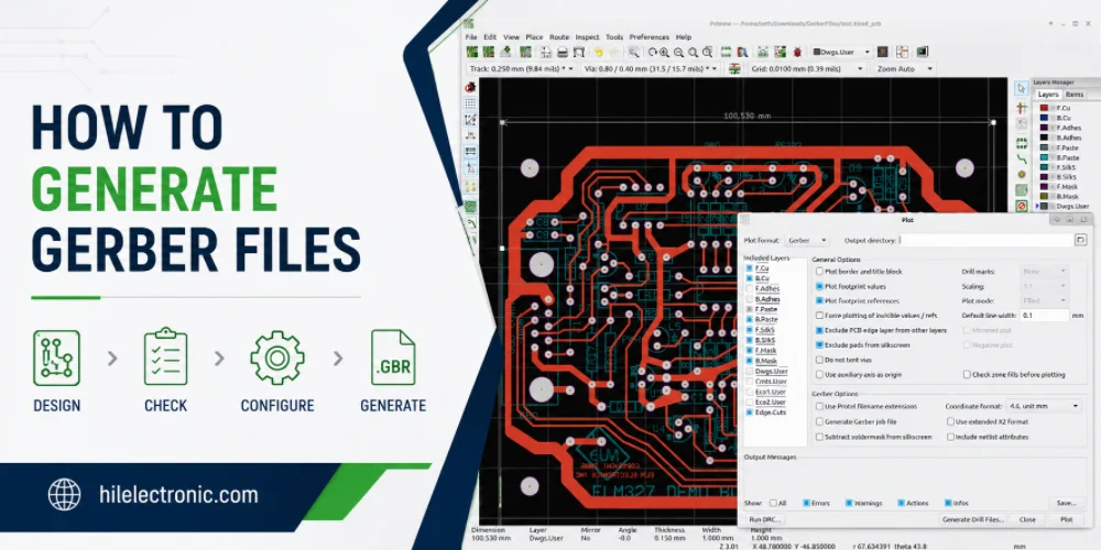
How to Generate Gerber Files for PCB Manufacturing
Figure 1. how to generate Gerber files image for Highleap...
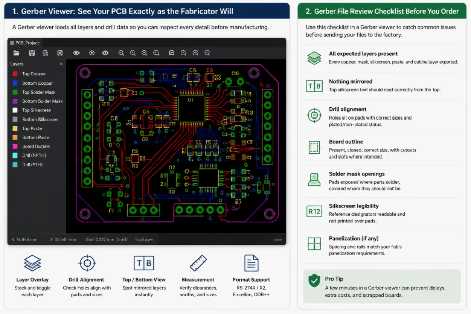
Gerber File Review Checklist: How to Check PCB Files Before You Order
Figure 1. Gerber file review catches missing layers, drill...
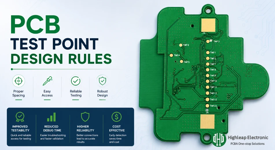
PCB Test Point Design Rules for Debug and ICT
Figure 1. PCB test point design rules help make debugging,...
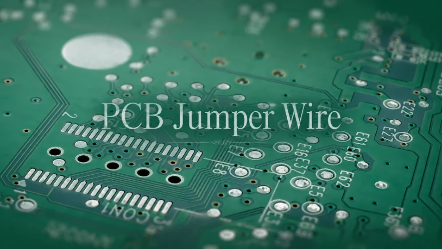
PCB Jumper Wire: Uses, Types, and Design Tips
Figure 1. PCB jumper wires are useful for prototypes and...
How to get a quote for PCBs
Let us run DFM/DFA analysis for you and get back to you with a report.
You can upload your files securely through our website.
We require the following information in order to give you a quote:
-
- Gerber, ODB++, or .pcb, spec.
- BOM list if you require assembly
- Quantity
- Turn time
In addition to PCB manufacturing, we offer a comprehensive range of electronic services, including PCB design, PCBA (Printed Circuit Board Assembly), and turnkey solutions. Whether you need help with prototyping, design verification, component sourcing, or mass production, we provide end-to-end support to ensure your project’s success. For PCBA services, please provide your BOM (Bill of Materials) and any specific assembly instructions. We also offer DFM/DFA analysis to optimize your designs for manufacturability and assembly, ensuring a smooth production process.