
Red PCB Manufacturing: Complete Guide to Red Solder Mask PCB Technology

At Highleap Electronics, we specialize in manufacturing high-performance red PCBs that combine striking aesthetics with exceptional functionality. Red solder mask technology offers unique advantages for specific applications, from automotive electronics to IoT devices. This comprehensive guide explores everything you need to know about red PCB technology and its applications. Get professional red PCB manufacturing services with custom solder mask solutions. Fast delivery, competitive pricing, and superior quality guaranteed.
Table of Contents
- What is Red PCB?
- Red Solder Mask Technology
- Benefits of Red PCB
- Red PCB vs Other Colors
- Applications and Industries
- Manufacturing Process
- Design Considerations
- Cost Analysis
- Conclusion
What is Red PCB?
A Red PCB is a printed circuit board featuring a distinctive red solder mask layer that provides both protective and aesthetic benefits. The red color comes from specialized pigments mixed into the solder resist material, creating a vibrant appearance while maintaining all the protective qualities of traditional solder masks. Understanding different PCB solder mask colors helps engineers select the optimal choice for specific applications.

Key Characteristics of Red PCB
The red solder mask technology offers several distinctive features:
- High visibility for component placement and inspection
- Excellent contrast with white silkscreen markings
- Professional appearance in consumer electronics
- Good heat dissipation properties
- UV stability for long-term color retention
Unlike traditional green PCBs, red PCBs provide a unique combination of functionality and visual appeal that makes them ideal for products where aesthetics matter.
Red Solder Mask Technology
Composition and Properties
Red solder mask is composed of epoxy-based polymers mixed with red pigments and photoinitiators. The formulation provides exceptional performance across multiple parameters:
Chemical Properties
Physical Properties
• Thickness range: 0.012-0.025mm (0.5-1.0 mil)
• Adhesion strength: >1.5 kg/cm
• Hardness: 6H pencil hardness
• Color stability: <2 ΔE after 1000 hours UV exposure
Manufacturing Standards
Our red PCBs meet or exceed industry standards:
- IPC-SM-840D Class H specifications
- RoHS and REACH compliant materials
- UL certification for flame resistance
- ISO 9001:2015 quality management
- IPC-A-600 Class 2 and Class 3 acceptability
Benefits of Red PCB
1. Enhanced Visual Inspection
Red solder mask provides superior visibility for quality control:
- 35% faster defect detection compared to darker colors
- Reduced eye strain during manual inspection
- Better contrast for automated optical inspection (AOI)
- Clear visibility of trace patterns and vias
2. Aesthetic Appeal
Red PCBs offer distinct visual advantages:
- Premium appearance in transparent enclosures
- Brand differentiation in competitive markets
- Color coordination with product design themes
- Professional look for high-end electronics
3. Functional Advantages
Beyond aesthetics, red PCBs provide practical benefits:
- Moderate heat absorption – better than black, similar to green
- Excellent silkscreen visibility with white ink
- Good chemical resistance to flux and cleaning agents
- Stable electrical properties across temperature ranges
4. Market Differentiation
Red PCBs help products stand out:
- Unique identification in multi-board systems
- Enhanced perceived value in consumer products
- Easy troubleshooting with clear component visibility
- Brand consistency for companies with red color themes
Red PCB vs Other Colors
Red PCB
Cost Premium: +3-8%
Visual Inspection: Very Good
Heat Absorption: Medium
Best For: Consumer electronics, IoT devices
Green PCB
Cost Premium: Baseline
Visual Inspection: Good
Heat Absorption: Medium
Best For: General purpose, cost-sensitive
Black PCB
Cost Premium: +5-10%
Visual Inspection: Poor
Heat Absorption: High
Best For: Gaming, premium products
Blue PCB
Cost Premium: +5-8%
Visual Inspection: Good
Heat Absorption: Medium
Best For: Prototyping, professional
Yellow PCB
Cost Premium: +5-10%
Visual Inspection: Excellent
Heat Absorption: Low
Best For: Industrial, high visibility
Selection Criteria
Choose Red PCB when:
- Product design requires red aesthetics
- Clear component visibility is important
- Brand identity includes red color schemes
- Differentiation from competitors matters
- Working with IoT or consumer electronics
Consider alternatives when:
- Lowest cost is critical (choose green)
- Maximum heat dissipation needed (choose white)
- Stealth appearance required (choose black)
- Prototyping or development (choose blue)
Applications and Industries

Consumer Electronics
Red PCBs excel in consumer applications:
- Gaming Peripherals: RGB keyboards, gaming mice, controllers
- Audio Equipment: Amplifiers, DACs, mixing consoles
- Smart Home: IoT devices, smart speakers, home automation
- Wearables: Fitness trackers, smartwatches
Automotive Electronics
The automotive industry increasingly uses red PCBs:
- Infotainment Systems: Display modules, control units
- LED Lighting: Interior ambient lighting, dashboard illumination
- Safety Systems: ADAS modules, parking sensors
- Electric Vehicles: Battery management systems, charging controllers
Industrial Applications
Red PCBs serve various industrial needs:
- Test Equipment: Measurement instruments, oscilloscopes
- Control Systems: PLCs, HMI interfaces
- Power Electronics: Inverters, motor controllers
- Safety Devices: Emergency stop circuits, alarm systems
IoT and Communications
Modern connectivity solutions utilize red PCBs:
- Wireless Modules: WiFi, Bluetooth, LoRa devices
- Sensor Networks: Environmental monitoring, smart city infrastructure
- Edge Computing: Gateway devices, data loggers
- 5G Equipment: Small cells, antenna systems
Manufacturing Process

Step-by-Step Production
Our PCB fabrication process for red PCBs includes:
1. Substrate Preparation
- FR-4 material cutting and drilling
- Surface cleaning and deburring
- Copper plating for through-holes
- Pattern transfer preparation
2. Circuit Formation
- Photoresist application
- UV exposure with circuit pattern
- Developing and etching
- Copper trace inspection
3. Red Solder Mask Application
- Surface preparation and cleaning
- Red solder mask coating (screen printing or spray)
- UV exposure through mask artwork
- Developing to remove unexposed areas
- Final curing at 150°C for 60 minutes
4. Surface Finish
- HASL, ENIG, or OSP application
- Silkscreen printing (typically white)
- Electrical testing and AOI
- Final quality inspection
Quality Control Measures
Our Quality Standards
✓ 100% Electrical Testing
Full connectivity verification
✓ AOI Inspection
Multiple stage verification
✓ Cross-Section Analysis
Layer registration check
✓ Contamination Testing
IPC standard compliance
Design Guidelines
PCB Layout Considerations
Trace Design:
- Signal traces: Minimum 0.1mm (4 mil) width
- Power traces: Calculate using IPC-2221 standards
- Spacing: Minimum 0.1mm (4 mil) between traces
- Via sizing: 0.2mm (8 mil) minimum drill size
Component Placement:
- Add fiducial markers for PCB assembly
- Maintain 0.5mm clearance from board edge
- Consider red background for LED indicators
- Group components by function and height
Silkscreen Optimization
Best Practices for Red PCB Silkscreen
- Use white silkscreen for maximum contrast (ΔE > 70)
- Minimum text height: 0.8mm (32 mil)
- Line width: Minimum 0.15mm (6 mil)
- Avoid yellow or orange silkscreen on red
- Include polarity markers and reference designators
Solder Mask Requirements
Design specifications:
- Solder mask clearance: Pad size + 0.05mm (2 mil)
- Minimum web width: 0.075mm (3 mil)
- Via tenting: 0.1mm (4 mil) annular ring coverage
- Solder dam: Minimum 0.1mm (4 mil) between pads
Thermal Management
Red PCBs require thermal considerations:
- Thermal vias: Use for heat dissipation
- Copper pour: Implement ground planes
- Component spacing: Allow airflow between hot components
- Heat sinks: Design mounting points where needed
Cost Analysis

Pricing Factors
Red PCB costs depend on several variables:
Volume Pricing Structure
1-10 pieces
+8-10% premium
10-100 pieces
+5-8% premium
100-1000 pieces
+3-5% premium
1000+ pieces
+2-3% premium
Additional Cost Factors:
- Board complexity: Layer count, via density
- Surface finish: HASL < OSP < ENIG < Hard Gold
- Lead time: Standard (5-7 days) vs expedited (24-48 hours)
- Special requirements: Impedance control, blind/buried vias
ROI Considerations
Value Proposition
- Brand premium: 10-15% higher product pricing potential
- Inspection efficiency: 20% faster QC process
- Quality improvement: 15% reduction in assembly errors
- Customer satisfaction: Enhanced perceived quality
Our electronic manufacturing service team can help optimize your design for cost-effectiveness while maintaining quality standards.
Conclusion
Red PCBs offer an exceptional combination of functionality and visual appeal that makes them ideal for modern electronic applications. The distinctive red solder mask not only provides superior contrast for inspection and professional aesthetics but also delivers reliable performance across automotive, consumer electronics, and IoT applications. At Highleap Electronics, our advanced PCB fabrication and PCB assembly capabilities ensure your red PCB projects achieve optimal quality while maintaining cost efficiency.
Whether you’re developing products that require brand differentiation, enhanced visibility for quality control, or simply want to stand out in the market, red PCB technology provides the perfect solution. The modest cost premium of 3-8% is easily justified by improved inspection efficiency, reduced defect rates, and enhanced product appeal. Contact our engineering team today to discover how red solder mask technology can elevate your next electronics project.

Related Articles
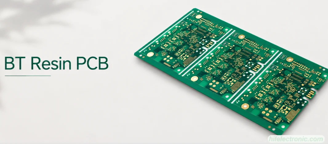
BT Resin PCB: Properties, Uses, and Fabrication Controls
Figure 1. BT resin PCB image for PCB manufacturing...
PCB Potting Services: Compounds, Process, and Design Rules
Figure 1. PCB potting services image for Highleap...
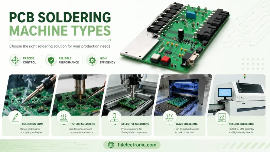
PCB Soldering Machine Types: Reflow, Wave, and Selective Equipment
Figure 1. PCB soldering machine types image for Highleap...

Clean Flux vs No-Clean Flux: Residue, Cleaning, and PCB Reliability
Figure 1. clean flux vs no-clean flux image for Highleap...
How to get a quote for PCBs
Let us run DFM/DFA analysis for you and get back to you with a report.
You can upload your files securely through our website.
We require the following information in order to give you a quote:
-
- Gerber, ODB++, or .pcb, spec.
- BOM list if you require assembly
- Quantity
- Turn time
In addition to PCB manufacturing, we offer a comprehensive range of electronic services, including PCB design, PCBA (Printed Circuit Board Assembly), and turnkey solutions. Whether you need help with prototyping, design verification, component sourcing, or mass production, we provide end-to-end support to ensure your project’s success. For PCBA services, please provide your BOM (Bill of Materials) and any specific assembly instructions. We also offer DFM/DFA analysis to optimize your designs for manufacturability and assembly, ensuring a smooth production process.