
Precision Press Fit PCB Manufacturing with Tight Tolerances
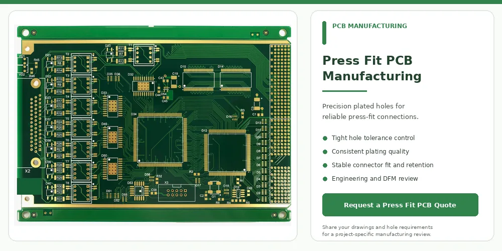
Press-fit PCB manufacturing requires close coordination between the PCB fabrication specification and the selected connector’s application requirements. A compliant pin forms an electrical connection through mechanical interference with a plated through-hole (PTH), so finished-hole diameter and tolerance, hole-wall copper, board thickness and connector geometry must meet the approved specifications. Highleap Electronics supports PCB manufacturing and assembly projects with a focus on reviewing these requirements before production release.
For a manufacturing quote, provide the PCB fabrication files, connector part number, application drawing, finished-hole specifications and order quantity. Highleap Electronics can review the available documentation and confirm the applicable manufacturing scope. Dedicated press-fit insertion equipment and specialized qualification tests must be confirmed separately before they are included in a project proposal.
Table of contents
PRESS FIT PCB PROJECT
Send your fabrication data, connector details and production quantity for a project-specific review.
Press Fit PCB Manufacturing Requirements
Press-fit PCB manufacturing begins with the connector’s approved application requirements. The board must provide the specified plated holes, copper geometry and mechanical dimensions so that the connector can be installed without relying on assumptions about the fit between the pin and the PCB.
For a manufacturer, the critical task is to translate the released design and connector documentation into a manufacturable board construction. A nominal hole dimension on its own may be insufficient if the drawing does not clarify whether it refers to the pre-plating drill diameter or the finished-hole diameter.
The manufacturing review should address the following points:
- Finished-hole diameter: Confirm the specified diameter range and tolerance against the connector manufacturer’s application documentation.
- Plated through-hole construction: Identify the required hole-wall copper, plating acceptance criteria and relevant hole-wall quality requirements.
- Pad and annular-ring geometry: Check the relationship between the finished hole, surrounding pad, internal copper connections and adjacent features.
- Board thickness and stackup: Confirm the finished thickness and layer construction against the approved connector requirements.
- Connector layout: Review pin pitch, hole positions, connector orientation, mounting features, slots and board-edge clearances.
- Material and operating conditions: Identify any specified thermal, environmental or reliability requirements that affect the board construction.
These parameters are related. For example, a change to the hole diameter can affect the intended mechanical interference, while a change to pad geometry may reduce the available annular ring or alter copper clearances. Such changes should be evaluated against the complete design and approved by the customer before manufacturing release.
Press-fit compatibility should not be inferred from the fact that a board can be drilled and plated. It must be assessed against the selected connector, its approved hole-size range and the applicable fabrication specification. The manufacturing route should reflect the actual board requirements rather than a generic press-fit specification.
When reviewing a quotation, distinguish the bare PCB from any subsequent connector installation. The fabrication scope covers the board and its specified features; connector insertion introduces additional equipment, process and acceptance requirements. Highleap’s bare-board manufacturing process is the relevant starting point for defining the PCB construction, while any dedicated press-fit assembly scope must be confirmed separately.
Press Fit Hole Size Tolerances and Plating
Finished-hole dimensions are among the most important parameters in a press-fit design. A compliant pin is engineered to work within a defined range of hole dimensions. If the finished hole falls outside that range, the resulting interference may differ from the intended design and could affect insertion force, electrical contact or the mechanical condition of the plated hole.
There is no single finished-hole diameter or tolerance suitable for every press-fit connector. The correct value comes from the selected connector’s application specification and the agreed PCB drawing.
Drill Diameter Versus Finished-Hole Diameter
The drill diameter describes the hole produced before subsequent metallization. The finished-hole diameter describes the completed hole according to the drawing’s measurement definition. Because fabrication and plating affect the final dimensions, the two values should not be treated as interchangeable.
Before releasing a press-fit PCB for production, confirm:
- The connector-approved finished-hole diameter range.
- The dimensional tolerance and the method used to define or measure the finished hole.
- Whether the specified hole is a plated through-hole and which plating requirements apply.
- The hole-position tolerance and any relevant datum references.
- The required inspection method, sampling plan and reporting requirements.
The connector pin’s nominal dimension alone is not enough to determine the appropriate drill size. The application drawing should establish the permitted finished-hole range and any additional requirements for board thickness, plating and assembly.
The distinction also matters during engineering changes. A drill-size adjustment should not be made simply to compensate for an assumed plating allowance. The manufacturer must evaluate the approved finished-hole requirement and the applicable fabrication process together. Where the drawing is incomplete, the missing information should be resolved before the production data is finalized.
Hole-Wall Copper and Plating Requirements
During insertion, the compliant pin applies mechanical force to the plated-hole interface. The hole-wall copper and surrounding PCB structure must therefore meet the requirements specified for the connector and application. Relevant considerations may include plating thickness, continuity, hole-wall condition and the integrity of the surrounding copper features.
The required copper thickness should come from the applicable PCB specification, connector documentation and customer drawing. It should not be assumed that every press-fit design uses the same copper thickness or that a conventional plated-through-hole specification automatically covers every press-fit requirement.
Other manufacturing considerations include:
- Plating continuity: The finished hole must meet the specified requirements for electrical continuity and hole-wall integrity.
- Annular ring: The design must preserve the required copper around the hole while maintaining clearances to adjacent conductors.
- Hole-wall condition: Relevant manufacturing defects must be assessed against the agreed acceptance criteria.
- Dimensional stability: Board thickness, laminate properties and the surrounding construction should be considered where they affect the approved connector interface.
- Surface finish: The selected finish must be compatible with the board design and application. A finish specified for solderable pads does not, by itself, define the press-fit hole requirements.
Drilling and metallization should be evaluated as part of the same manufacturing sequence. The finished dimensions and hole quality must be consistent with the approved specification, rather than determined from a generic drill-size rule. For the process details, see drilling and finished-hole dimensions.
DFM Review Before Production Release
A useful DFM review considers the connector interface alongside the surrounding layout. This may include hole-to-pad relationships, internal copper clearances, connector pitch, board-edge distance, mounting features, slots and mechanical support. On multilayer boards, the review should also consider how the holes connect to internal copper layers and whether the required clearances can be maintained.
If the connector specification, hole tolerance or plating requirements are incomplete, those gaps should be identified before the fabrication data is released. A proposed change to the hole diameter, pad geometry or copper clearance should be approved by the customer rather than silently incorporated into the manufacturing files.
For this reason, it is worth taking time to review the fabrication data before release, especially when the design contains dense connector layouts or tight mechanical tolerances. This review helps identify manufacturing questions, but it does not replace connector qualification or application-specific reliability testing.
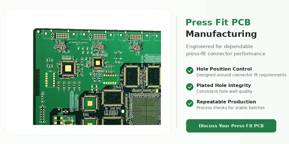
Press Fit PCB
Press Fit PCB Assembly and Connector Integration
Press-fit PCB assembly involves installing a compatible connector into the prepared PCB holes using an appropriate mechanical insertion process. Unlike conventional soldering, the compliant-pin connection is designed to establish electrical contact through the specified interference between the pin and the plated hole.
The connector and PCB must be compatible before assembly begins. Hole dimensions, pin configuration, board thickness, support fixtures and insertion conditions should align with the connector manufacturer’s documentation and the project’s approved requirements.
Press Fit Versus Through-Hole Soldering
Both methods use component leads or pins that pass through PCB holes, but they form the connection differently. Press-fit technology relies on the mechanical and electrical interface between the compliant pin and the plated hole. Conventional soldered connections rely on the specified solder joint.
| Comparison | Press Fit | Through-Hole Soldering |
|---|---|---|
| Connection mechanism | Mechanical interference and electrical contact between the compliant pin and plated hole. | Electrical and mechanical connection through the specified solder joint. |
| Critical PCB requirement | Connector-approved finished-hole dimensions and suitable plated-hole construction. | Hole, pad and component geometry appropriate for the specified soldering process. |
| Assembly process | Controlled mechanical insertion using an appropriate method and fixture. | Soldering using an approved process and applicable joint acceptance criteria. |
| Inspection focus | Connector seating, PCB integrity and specified electrical or mechanical verification. | Solder-joint quality, wetting, hole fill where applicable and electrical verification. |
Neither method is universally better. The right choice depends on the connector design, operating environment, product requirements, serviceability and total manufacturing cost. A board may also combine press-fit connectors with SMT components and conventionally soldered through-hole parts.
Where a soldered connection is specified, the requirements differ from those of a compliant-pin interface. The process should follow the approved design rather than substituting one connection method for another without engineering approval. For a closer look at the alternative, see conventional through-hole soldering.
What Must Be Confirmed Before Connector Insertion?
Before a press-fit connector is installed, the project team should confirm the connector part number, approved hole specification, PCB revision and assembly instructions. If the board contains multiple connector types, each interface may need its own verification.
The assembly plan should also define the applicable mechanical and inspection requirements, which may include:
- Connector positioning: Correct orientation, alignment, pin mapping and seating position.
- Fixture and support: Appropriate PCB support during insertion to reduce the risk of bending or localized damage.
- Insertion conditions: The approved insertion method and any specified force or process-monitoring requirements.
- Post-assembly inspection: Connector seating, visible PCB damage, electrical continuity and other agreed acceptance checks.
- Traceability: Connector lot, PCB revision, assembly records and inspection documentation where required.
These are planning considerations, not a claim that every project automatically includes every listed test. Equipment, process monitoring, sampling and acceptance documentation must be confirmed before the order is placed.
When the product includes other electronic components, component assembly can be planned alongside the bare board. However, standard SMT or through-hole assembly should not be treated as proof that a supplier can perform dedicated press-fit insertion. The available equipment, connector requirements and verification scope must be confirmed before this operation is included in the quotation.
Press Fit PCB Quality Control and Cost
Press-fit PCB quality control should reflect the failure risks and acceptance requirements of the specific connector interface. A continuity or isolation test can verify aspects of electrical connectivity, but it does not by itself establish that a press-fit connection meets every mechanical, dimensional or long-term reliability requirement.
Inspection and Verification
The inspection plan should be agreed before production. Depending on the application, the following checks may be relevant:
- Finished-hole dimensions: Verify the specified hole size and tolerance using the agreed measurement method and sampling plan.
- Plated-hole integrity: Assess the required plating condition, continuity and hole-wall acceptance criteria.
- PCB dimensional inspection: Confirm connector-hole positions, board outline, thickness and other critical mechanical dimensions.
- Electrical testing: Perform the specified continuity and isolation checks, with additional electrical verification where required.
- Post-assembly inspection: Check connector seating, PCB condition and the defined acceptance criteria for the assembled interface.
- Additional qualification: Apply insertion-force, retention-force, contact-resistance, microsection or other verification methods when required by the connector specification or customer acceptance plan.
For high-reliability applications, the customer may specify additional qualification and documentation. IPC-9797A addresses press-fit technology characterization, qualification and acceptance for automotive and other high-reliability applications. Where this standard is required, the applicable revision, scope and acceptance requirements should be agreed for the project.
Specialized tests may require dedicated equipment, fixtures, samples or external laboratory support. They should not be assumed to be included in a standard PCB fabrication quotation. The scope and availability of each test must be confirmed before production.
What Affects Press Fit PCB Cost?
The cost of a press-fit PCB depends on the board construction, connector interface requirements, manufacturing quantity and inspection scope. The presence of press-fit holes alone is not enough to calculate an accurate price.
The main cost drivers include:
- PCB layer count and construction: Layer count, board thickness, laminate selection and special stackup requirements.
- Hole dimensions and tolerances: Finished-hole size, positional requirements and the manufacturing controls needed to meet the drawing.
- Plating specifications: Required hole-wall copper, plating acceptance criteria and any special material or finish requirements.
- Board geometry: Connector density, board outline, slots, cutouts, tight mechanical features and panelization requirements.
- Quantity and production planning: Prototype quantity, repeat production volume, tooling requirements and panel utilization.
- Inspection and qualification: Dimensional reports, microsections, special tests, documentation and customer-defined acceptance criteria.
- Assembly scope: Connector sourcing, insertion, fixtures, inspection and additional assembly work, if included and confirmed as available.
Lead time depends on the approved fabrication route, material availability, order quantity, inspection requirements and any additional qualification work. A project-specific delivery estimate should be confirmed after the technical requirements have been reviewed.
When comparing quotations, review the assumptions behind the price as well as the total. A proposal based on standard plated through-holes may not be comparable to one that includes tighter dimensional controls, specialized inspection or connector insertion. For a broader view of other factors in bare-board pricing, compare the complete fabrication specifications rather than layer count alone.
Press Fit PCB Manufacturing Quote and RFQ
To obtain a meaningful quotation, provide the latest fabrication files together with the connector manufacturer’s application information. These documents help establish whether the finished-hole dimensions, plating requirements, PCB construction and proposed assembly method are compatible with the intended connector.
If the design is still under development, preliminary files can help identify unresolved questions. Clearly mark any open items involving connector selection, finished-hole tolerances, board thickness, plating or assembly requirements so they can be reviewed before the manufacturing specification is released.
Press Fit PCB RFQ Checklist
- PCB fabrication files: Gerber X2 or ODB++ data, NC drill files, board outline and fabrication drawing.
- PCB construction: Layer count, stackup, laminate requirements, finished board thickness and copper specifications.
- Connector information: Manufacturer, complete part number, application drawing and approved press-fit hole requirements.
- Hole specifications: Finished-hole diameter and tolerance, hole position, plating requirements and relevant dimensional datums.
- Mechanical requirements: Connector pitch, board-edge distances, mounting features, slots and other critical dimensions.
- Quality requirements: Applicable IPC revision and acceptance class, inspection methods, dimensional reports and special qualification criteria.
- Commercial details: Prototype or production quantity, required delivery date, packaging and shipping requirements.
- Assembly requirements: Connector BOM, assembly drawing, component supply responsibility, insertion requirements and inspection scope if assembly is requested.
Providing these details at the beginning helps prevent quotations from being based on different assumptions. If the connector part number or hole specification has not been finalized, state this clearly so the missing information can be identified before manufacturing release.
Define the Manufacturing Scope Before Ordering
Highleap Electronics works with customers on PCB manufacturing and assembly requirements. The appropriate project scope depends on whether the inquiry covers bare PCBs with press-fit interfaces, component assembly, or a combined manufacturing solution. Dedicated press-fit insertion and specialized verification must be confirmed against the required process and equipment before they are included in the quotation.
For an accurate proposal, identify whether you need bare-board fabrication only or whether the order also includes connector sourcing, insertion and post-assembly verification. This distinction allows the technical requirements, inspection scope and commercial proposal to be evaluated consistently.
PRESS FIT PCB PROJECT
Discuss Your Press Fit PCB Requirements
Send your fabrication files, connector specifications, finished-hole requirements and order quantity to Highleap Electronics. The project can then be reviewed against the required manufacturing and quotation scope.
Pricing and lead time confirmed after engineering review.
For the fastest and most accurate review, include the connector part number and the approved finished-hole specification with your inquiry. If dedicated press-fit assembly or specialized qualification is required, identify it explicitly so the necessary equipment, process and inspection requirements can be confirmed before the order is placed.

Recommended Posts
Optical Transceiver PCB Assembly Services in China
Highleap Electronics provides optical transceiver PCB...
8 Layer HDI PCB Manufacturer in China
Highleap Electronics provides 8 layer HDI PCB...
8 Layer Rigid-Flex PCB Manufacturing and Cost Guide
An 8 layer rigid-flex PCB combines multilayer rigid...
8 Layer PCB Cost in China: Rigid, Flexible & Rigid-Flex Pricing
How much does an 8 layer PCB cost? The answer depends on...
How to get a quote for PCBs
Let‘s run DFM/DFA analysis for you and get back to you with a report. You can upload your files securely through our website. We require the following information in order to give you a quote:
-
- Gerber, ODB++, or .pcb, spec.
- BOM list if you require assembly
- Quantity
- Turn time
In addition to PCB manufacturing, we offer a comprehensive range of electronic services, including PCB design, PCBA, and turnkey solutions. Whether you need help with prototyping, design verification, component sourcing, or mass production, we provide end-to-end support to ensure your project’s success.
For PCBA services, please provide your BOM (Bill of Materials) and any specific assembly instructions. We also offer DFM/DFA analysis to optimize your designs for manufacturability and assembly, ensuring a smooth production process.