
Optical Transceiver PCB Manufacturer for Custom Pluggable Modules
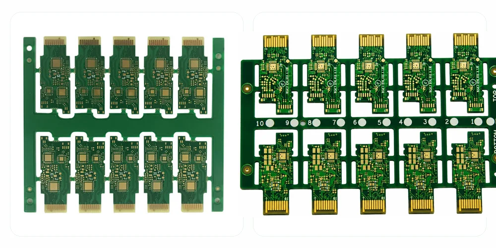
Highleap Electronics manufactures and assembles custom optical transceiver PCBs for OEMs, optical-module developers and electronics manufacturers sourcing boards for SFP-family, QSFP-family, QSFP-DD, OSFP and proprietary transceiver products. We work with customer-released designs and module drawings to supply bare PCBs or populated PCB assemblies, with the fabrication and assembly scope defined separately in the quotation.
These are compact, production-critical boards. A delivered PCB must do more than pass electrical continuity testing: the finished card edge must fit its connector, the board outline must fit the module housing, the laminate and stackup must match the electrical specification, and the surface finish must support both component soldering and repeated connector mating where required. Highleap coordinates these requirements during engineering review and manufacturing release, rather than quoting an optical-transceiver board from its layer count alone.
Our production scope includes multilayer rigid PCB fabrication, high-density interconnect features, controlled-impedance processing, specified contact finishes, SMT assembly and production inspection. For a project quotation, send the board data, mechanical drawing, stackup, quantity and—if assembly is required—the BOM and assembly documentation.
Table of contents
- Custom Optical Transceiver PCB Supply for OEM and Module Programs
- Multilayer and HDI PCB Construction for Dense Transceiver Boards
- Card-Edge Contacts, Gold Plating and Precision Mechanical Features
- Optical Transceiver PCB Assembly and Manufacturing Coordination
- Prototype Qualification, Lot Consistency and Delivery Control
- Request Custom Optical Transceiver PCB Manufacturing or Assembly
CUSTOM OPTICAL TRANSCEIVER PCB
Sourcing Custom Transceiver PCBs?
Share your board stackup, contact drawing, production quantities and PCB files for a project-specific manufacturing or assembly quotation.
Request a Transceiver PCB Quote →Custom Optical Transceiver PCB Supply for OEM and Module Programs
Highleap supplies boards against the customer’s controlled design, rather than offering one interchangeable PCB for every transceiver format. A QSFP-DD design with a specific host-edge geometry, package layout and heat-spreader arrangement cannot be replaced by a nominally similar board simply because it uses the same aggregate data rate. Our scope begins with identifying the exact PCB revision and the features that determine interchangeability within the intended product.
Typical inquiries include a newly released module PCB moving from engineering prototypes to production, an existing design being transferred to a second manufacturing source, or a board that needs improved cost and delivery stability after a material or component change. For a new program, we review the fabrication package and highlight manufacturing questions that should be resolved before tooling. For a source-transfer project, we can compare the released drawings, previous manufacturing requirements and acceptance records against the proposed production route.
| Project type | Important information for our quotation | Production focus |
|---|---|---|
| SFP / SFP+ / SFP28 PCB | Outline and board thickness, edge-contact drawing, component keep-outs | Mechanical fit, contact finish, stable small-board processing |
| QSFP / QSFP28 / QSFP-DD PCB | Exact form-factor revision, contact layout, multilayer stackup, critical components | Dense routing, HDI requirements, controlled dimensions |
| OSFP PCB | Housing datum drawing, host-contact requirements, thermal interface and thickness limits | Card-edge consistency, board flatness and assembly clearance |
| Custom optical transceiver PCB | Full mechanical package, controlled files, test and inspection requirements | Custom fabrication route, special-process qualification and repeatability |
We do not assume the form factor determines a fixed copper-layer count, dielectric material or microvia arrangement. The actual approved design drives the build. Customers working across several optical-module platforms can also use our optical module PCB manufacturing program for fabrication coordination by platform and production specification.
Production Release for a New Module Versus a Source Transfer
A new OEM board and a repeat-production transfer do not enter our production workflow with the same information. A new module program typically has an approved electrical design but still needs its fabrication output checked against the housing drawing, card-edge specification, laminate availability and the assembler’s process plan. We begin by matching the revision on the fabrication data to the revision on the stackup, outline, contact plating drawing and purchase order. If an edge-contact finish is shown only on an informal assembly drawing, that requirement is raised before fabrication is scheduled.
A supplier-transfer order usually carries a second obligation: preserve the features previously qualified by the customer. A technically similar laminate is not automatically an approved replacement, especially where channel insertion loss and dielectric construction are controlled. Likewise, changing the finished board thickness or the gold-contact process can affect connector mating even if the overall outline remains unchanged. We therefore request the controlled acceptance drawing, approved alternates and any first-article requirements that need to travel with the design. These documents set the boundaries of an acceptable quotation, rather than being treated as optional paperwork.
What Can Be Combined Under One Highleap Order
Customers can order the bare PCB alone or request coordinated fabrication and populated-board production. A combined project uses the same released PCB revision across board fabrication, component sourcing and SMT planning, while retaining separate quality checkpoints for the bare board and PCBA. Where customers supply components or require a specific test fixture, that supply responsibility and test scope appear in the order documents. We avoid describing optical engine assembly, active optical alignment or full-module qualification as part of an ordinary PCBA delivery unless a separate service scope has been confirmed.
Multilayer and HDI PCB Construction for Dense Transceiver Boards
Highleap Electronics fabricates multilayer optical transceiver PCBs to customer-released stackups, copper requirements and via maps. In a compact transceiver, the processing devices, power stages, management circuitry and connector contacts compete for the same limited area. A fabricator must therefore review feature geometry and layer interconnections as a combination, rather than approving an isolated trace width or drill size from a generic capability chart.
The manufacturing objective is a board whose impedance-sensitive conductors, fine-pitch escape routing and plated connections can be repeated across production panels. The manufacturing route is confirmed against the actual laminate, layer arrangement, finished thickness, copper weights and hole structure. Standard plated through-holes may be sufficient for one module; another approved design may require blind or buried vias, laser microvias or filled-and-capped via-in-pad. High-speed labeling alone does not establish which of these processes is necessary.
Key Multilayer and HDI Production Controls
-
Stackup and dielectric release: The approved drawing should identify each copper and dielectric layer, laminate grade, core/prepreg requirements, finished thickness and impedance targets. During CAM review, dielectric availability and expected finished copper are considered together; altering dielectric thickness merely to use available stock can invalidate a previously qualified channel. Material substitutions and electrical changes require the design owner’s written approval.
-
Fine-line imaging and etching: Minimum conductor width and spacing must be evaluated against copper weight, outer-layer plating, laminate behavior and etching compensation. A 2/2 mil feature may be manufacturable on a qualified process, but it should not become the default rule for ordinary routing. Demanding line geometry across many layers can tighten the process window, reduce yield and increase inspection or replacement-panel requirements.
-
Mechanical drilling and copper clearance: Drill-tool diameter, finished plated-hole diameter, board thickness and hole count are different cost and quality inputs. Smaller tools can slow drilling and make hole-wall plating more demanding, especially on a relatively thick multilayer board. Layer registration, internal nonfunctional pad removal where permitted, annular rings and drill-to-unconnected-copper clearance all require coordinated review; changing the drill diameter alone is not a complete DFM solution.
-
HDI and lamination sequencing: Laser microvias and blind/buried connections are mapped to particular layers before the fabrication sequence is approved. Additional drilling, registration, metallization and sequential lamination stages can change yield, price and lead time. Stacked structures require explicit material and reliability review; an HDI designation without a via cross-section or layer-connection map is insufficient for production release.
-
Via-in-pad finishing: An open via in a solderable fine-pitch pad can allow solder wicking. Ordinary solder-mask tenting or plugging does not automatically supply the flat plated surface needed for every BGA pad. Where the released design specifies filled, planarized and copper-capped vias, the quotation and traveler must account for filling, curing, leveling, cap plating and appropriate inspection. The required finish is coordinated with assembly before board manufacture.
-
Backdrilling and high-speed transitions: If via stubs are controlled by the signal budget, the design must define the affected nets, drill layers, permitted residual stub and acceptance method. Backdrilling is not a universal requirement for transceiver PCBs, and a production team cannot infer its depth from the aggregate data rate. Any proposed change in interconnect geometry is approved against the customer’s electrical performance requirements.
Manufacturing Sign-Off Before the Production Panel Is Released
The combination of laminate, trace geometry, drilled interconnections and acceptance tests matters more than any headline minimum-feature number. Highleap can flag manufacturing exceptions in its review and seek approval for alternatives before tooling or material commitments are finalized. For related process capability and inspection context, see high-speed PCB manufacturing and the separate optical transceiver bare-board fabrication service. Final capability depends on the submitted build and its complete feature combination.
Card-Edge Contacts, Gold Plating and Precision Mechanical Features
The host-facing edge of a pluggable optical transceiver PCB is a controlled electrical and mechanical interface. A board can pass electrical continuity testing yet fail to assemble because contact geometry, finished thickness, bevel location or outline datums do not agree with the mating housing and connector. Highleap reviews these features as part of the fabrication specification rather than treating the edge contacts as an ordinary surface-finish selection.
The contact finish also has a direct effect on quotation accuracy. ENIG on solderable component pads and specified selective hard-gold plating on mating contacts are different processing requirements. A purchase order that says only “gold finish” leaves the plating scope unclear and may trigger re-quoting once the connector drawing is reviewed. The full edge-interface drawing must identify where each finish is required and which dimensions are critical to fit.
Critical Card-Edge Manufacturing and Inspection Requirements
-
Selective contact plating: The drawing should define the plated-contact region, required finish type, underplate and gold thickness where specified, and the areas intentionally excluded from that process. Masking and selective plating can add operations beyond an ordinary ENIG board. The agreed acceptance method must match the actual wear-contact requirement rather than relying on the finished board’s general appearance.
-
Bevel and insertion geometry: Contact fingers may need a specified bevel, orientation and edge location relative to connector datums. The fabrication route must allow sufficient machining access and protect plated-contact areas. A rounded board outline or an unspecified “standard bevel” should not replace the connector manufacturer’s drawing, because even small geometry changes may affect insertion fit and contact performance.
-
Finished thickness at the mating region: The thickness shown on the stackup must be reconciled with the connector’s permitted engagement range, including any local finish or copper buildup considerations. Nominal thickness alone is not a guarantee of fit. Highleap can identify critical measurement locations and proposed inspection records before the design is released to fabrication.
-
Outline routing, slots and critical datums: Board edges, mounting features, small cutouts and connector alignment features must be controlled to the same revision as the copper data. A file set in which the Gerber outline contradicts the mechanical drawing is held for clarification. The acceptable routing tolerances and reference datums should be named instead of relying on unspecified general board tolerances.
-
Flatness and handling of thin modules: Short narrow boards can be sensitive to panel support, routing stress and local copper distribution. A proposed panel design considers handling and extraction without compromising the critical interface region. Where final bow/twist or flatness is a functional requirement, the test condition and allowable limit belong in the approved drawing; a generic “flat board” instruction cannot be measured consistently.
-
Inspection records and nonconformance decisions: Gold-contact finish, thickness, outline dimensions and bevel characteristics may require separate records depending on the customer specification. E-test alone cannot verify contact wear performance or mechanical fit. If the fabrication drawing and connector specification disagree, the manufacturing team requests a controlled decision rather than selecting the cheaper interpretation and shipping the board.
Release the Edge Interface as One Approved Specification
For repeat orders, the revision-controlled fabrication data, connector drawing, gold-finger specifications and accepted inspection method should remain together. A material or finish change may affect mechanical compatibility even if the copper artwork is unchanged. For a more detailed explanation of contact metallurgy, see Highleap’s gold-finger PCB manufacturing information. Any change that affects the interface is reviewed with the design owner before production resumes.
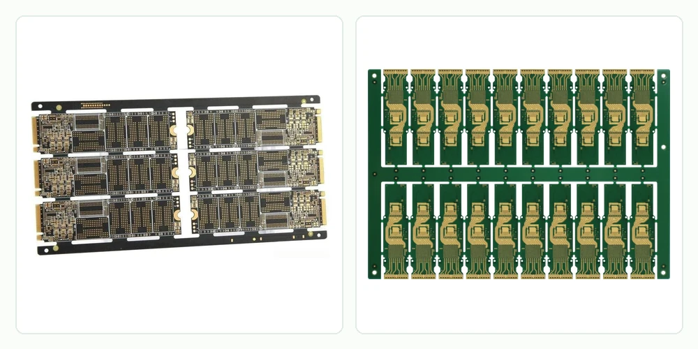
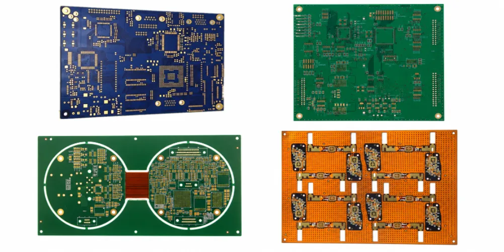
Optical transceiver PCB panels with fine-pitch component pads
Optical Transceiver PCB Assembly and Manufacturing Coordination
Highleap can provide bare-board fabrication alone or coordinate it with optical transceiver PCB assembly. When PCBA is included, the manufacturing handoff covers surface finish, SMT land patterns, via-in-pad treatment, assembly panel design and the availability of the specified components. This avoids a common source-transfer problem: a board that is manufacturable as bare PCB but creates soldering or handling problems on the approved assembly line.
For customer-defined PCBAs, the assembly scope can include component procurement, solder-paste printing, SMT placement and reflow, through-hole operations where required, AOI, X-ray for applicable hidden solder joints, and board-level electrical or functional testing where an approved procedure is available. Projects containing compact BGAs, QFNs, fine-pitch connectors or high-density passives receive package-specific process review. The BOM and assembly drawing must identify orientation, nonstandard part handling and any components that require special thermal profiles or protection during reflow.
Optical alignment, complete transceiver-module calibration, optical-power testing and bit-error-rate testing are not automatically part of bare-board or standard PCBA supply. They require a separately defined process, test equipment and acceptance scope. The full optical transceiver PCB assembly service addresses component sourcing, NPI, assembly and board-level deliverables in greater detail.
A combined fabrication and assembly RFQ can still be handled as a coordinated project while retaining separate acceptance milestones. Bare-board quality evidence establishes the PCB fabrication result; assembly inspection establishes placement and soldering quality; any module-level electrical/optical performance remains subject to the customer’s separate acceptance plan.
Fabrication Choices That Determine SMT Yield
When the requested deliverable is a populated transceiver board, Highleap connects fabrication review to assembly review before production release. Pad finish, solder-mask registration, via-in-pad planarity and the panel design affect paste printing and placement. A PCB that passes electrical test but has open vias in critical pads or insufficient mechanical support can create avoidable SMT defects. These risks are reviewed against the customer’s approved land pattern and component package data.
Assembly-sensitive features are identified specifically. For fine-pitch BGA or QFN devices, the process review can include stencil aperture strategy, component orientation, expected thermal mass, reflow sensitivity and access for inspection. If a low-loss or mixed-material laminate has different thermal behavior from standard FR-4, it should be assessed as part of the PCB-plus-assembly build rather than assuming identical reflow behavior. Changes that affect solderability or board support are approved at the appropriate engineering stage.
Separate Acceptance Gates for PCB, PCBA and Module
The delivered bare board can be measured for continuity, isolation, dimensions and agreed coupon results. Once assembled, component identity, placement, solder joints and the specified board-level electrical functions form a different acceptance gate. Complete transceiver optical performance—including optical coupling, receiver sensitivity, output power and BER—requires another test scope and, often, equipment beyond the normal PCBA line. A single order can coordinate these stages, but it should name which of them Highleap is contracted to deliver.
Prototype Qualification, Lot Consistency and Delivery Control
Highleap supports prototype, pilot and repeat-production PCB programs. The production approach for a first article differs from the approach for a recurring module order: the first batch must confirm the specified construction and the critical mechanical/electrical characteristics, while repeat orders must maintain the approved materials, processes, revision and inspection criteria. A supplier transfer should not treat a change of low-loss laminate, copper profile or contact plating as a silent commercial substitution.
Depending on the order specification, production controls may include inner-layer inspection, AOI, bare-board electrical test, critical dimensional measurements, plating or cross-section verification, and controlled-impedance coupons. The exact sample plan and acceptance class must be agreed in the order documentation. Test coupons can demonstrate a defined manufacturing property, but an impedance result alone does not certify the complete high-speed module channel.
For repeat production, we review forecast quantities, revision stability, approved alternates, material availability and lot-level documentation. If a design has critical surface-finish or insertion-edge requirements, those should appear as controlled characteristics in the production release. Packaging and handling can also matter for thin boards or contact-finish areas; the required protective method should be agreed before shipment rather than assumed.
The quotation stage is where unusual requirements should be exposed. Selective contact plating, via fill and cap, stringent material callouts, dedicated test reports and urgent delivery can introduce operations that were not included in a generic estimate. Highleap reviews these details before confirming price and the committed lead time, so the production plan reflects the board the customer actually ordered.
First-Article Evidence Versus Routine Batch Evidence
A first article should prove that the production route can make the features that actually control the module: contact thickness and plating, the board’s insertion edge, critical outline dimensions, specified impedance structures, internal via connections and finished material construction. The evidence is not the same for every program. Some orders need only standard inspection and bare-board electrical testing; others require dimensional reports, impedance coupons, microsection verification or customer-selected acceptance criteria. Highleap agrees on those outputs before production rather than presenting an unspecified “complete testing” claim.
A repeat order needs process discipline more than another generic qualification statement. Released Gerber and drill revisions, permitted laminate alternates, surface-finish requirements, approved panel drawing and inspection frequency should remain controlled. A supplier can still propose a process improvement, but changes affecting fit, electrical performance, solderability or acceptance evidence are reviewed before implementation. That is how prototype results remain meaningful when the order becomes a scheduled production program.
Supply Continuity During Revision Changes
A module customer may release a new BOM or housing revision without intentionally changing the PCB’s electrical design. That revision can nevertheless change pad geometry, contact position or thermal interfaces. Highleap requests clear revision identification and change notes to prevent old and new builds from being mixed. For repeat programs, shipment labels, lot references and protective packaging for plated contact areas can be specified as part of the delivery agreement. If the critical substrate becomes unavailable, an alternative is presented with its qualification implications instead of being silently substituted.
Request Custom Optical Transceiver PCB Manufacturing or Assembly
Send Highleap Electronics the latest Gerber/ODB++ data and drill files, a released stackup, board drawing, laminate and copper specifications, card-edge/contact-plating details, controlled-impedance requirements, and prototype or production quantities. If the module housing imposes special fit requirements, include the relevant mechanical reference drawing and the dimensions that must be verified. Specify inspection records, acceptance criteria and delivery destination where applicable.
Production-Ready RFQ Sequence
- Release the final Gerber/ODB++ and NC drill package, with the drawing and board revision.
- Provide the mating-contact layout, selective plating notes, critical outline and thickness tolerances.
- Identify fabrication quantity breaks and whether the deliverable is bare board or assembled PCBA.
- For PCBA, include approved BOM, placement data, programming and agreed inspection scope.
For populated boards, add a revision-controlled BOM with manufacturer part numbers, approved alternatives, centroid/pick-and-place files, assembly drawings, any programming files, and the required board-level test procedures. State clearly whether components are supplied by Highleap or consigned by the customer, and whether the requested deliverable is a bare PCB, an assembled PCBA or a separately qualified higher-level assembly.
Highleap can evaluate manufacturing feasibility, identify missing fabrication or assembly specifications, and quote the agreed work scope for prototype and recurring production. Submit your optical transceiver PCB files for a quotation with the target quantity and delivery requirements. A complete RFQ helps us quote the actual board construction and avoid avoidable changes after production release.
A Complete RFQ Reduces Repricing and Production Holds
The most useful fabrication package groups mechanical, electrical and finish requirements under one controlled revision. The board data establishes copper and drill geometry; the stackup establishes material and dielectric construction; the outline drawing establishes fit; and the finish specification establishes solderable pads and wear contacts. If any of these contradict one another, Highleap can raise an engineering question before confirming the commercial terms. Production quantities should include prototype and expected volume breaks, because material purchasing, panel utilization and inspection scope may change with order size.
For a combined PCBA request, the BOM should identify approved manufacturer part numbers and alternatives; the assembly files should state component orientation, special soldering constraints, programming and board-level test conditions. The quote can then distinguish bare-board fabrication, purchased components, assembly operations and optional tests. This provides a practical basis for evaluating unit price, tooling and lead time without confusing a PCBA offer with complete optical-module production.
CUSTOM OPTICAL TRANSCEIVER PCB
Sourcing Custom Transceiver PCBs?
Share your board stackup, contact drawing, production quantities and PCB files for a project-specific manufacturing or assembly quotation.
Pricing, process and schedule are confirmed after engineering review.

Recommended Posts
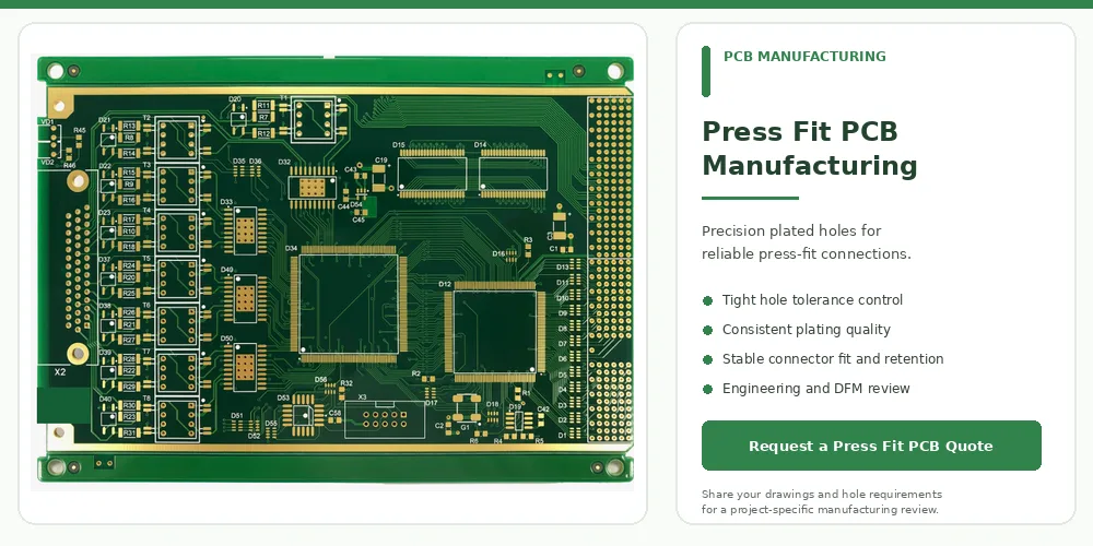
Precision Press Fit PCB Manufacturing with Tight Tolerances
Press-fit PCB manufacturing requires close coordination...
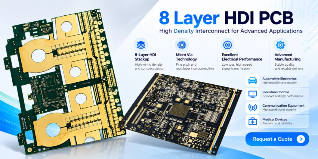
8 Layer HDI PCB Manufacturer in China
Highleap Electronics provides 8 layer HDI PCB...
8 Layer Rigid-Flex PCB Manufacturing and Cost Guide
An 8 layer rigid-flex PCB combines multilayer rigid...
8 Layer PCB Cost in China: Rigid, Flexible & Rigid-Flex Pricing
How much does an 8 layer PCB cost? The answer depends on...
How to get a quote for PCBs
Let‘s run DFM/DFA analysis for you and get back to you with a report. You can upload your files securely through our website. We require the following information in order to give you a quote:
-
- Gerber, ODB++, or .pcb, spec.
- BOM list if you require assembly
- Quantity
- Turn time
In addition to PCB manufacturing, we offer a comprehensive range of electronic services, including PCB design, PCBA, and turnkey solutions. Whether you need help with prototyping, design verification, component sourcing, or mass production, we provide end-to-end support to ensure your project’s success.
For PCBA services, please provide your BOM (Bill of Materials) and any specific assembly instructions. We also offer DFM/DFA analysis to optimize your designs for manufacturability and assembly, ensuring a smooth production process.