
Optical Module PCB Manufacturer for 400G, 800G and 1.6T Programs
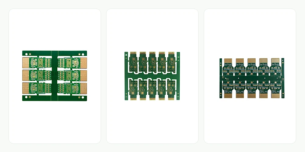
Highleap Electronics provides optical module PCB manufacturing and PCB assembly for customer-defined high-speed optical hardware. Our fabrication scope includes multilayer rigid PCBs, low-loss material systems, controlled-impedance circuitry, HDI interconnects, fine-line copper features, precision drilling and specified surface finishes. We support engineering builds, pilot orders and repeat production to an approved fabrication package rather than selling a generic board claimed to fit every optical-module platform.
For 400G, 800G and 1.6T development programs, high-speed requirements can make a seemingly small manufacturing change commercially significant. Laminate substitutions, copper-foil characteristics, dielectric tolerances, via structures and surface-finish processing can affect the released construction. Our engineering review aligns these requirements with a documented production route before Highleap confirms the order price, feasibility and delivery schedule.
Customers can request bare-board fabrication or a coordinated PCBA quotation. Supply the released design files, material and stackup schedule, defined signal and inspection requirements, expected volume and any assembly files so the quotation reflects the actual optical-module PCB.
Table of contents
- Optical Module PCB Production for Multiple Hardware Platforms
- Low-Loss PCB Materials, Stackup Control and Signal-Path Fabrication
- HDI, Microvias, Fine-Line Processing and Component Interface Features
- Optical Module PCB Dimensions, Surface Finishes and Mechanical Integration
- Manufacturing Verification and Repeat-Production Quality
- Request a Custom Optical Module PCB Manufacturing Quote
OPTICAL MODULE PCB FABRICATION
Planning an Optical Module PCB Build?
Send your released stackup, material requirements, via map and volume target for production review.
Request an Optical Module PCB Quote →Optical Module PCB Production for Multiple Hardware Platforms
Highleap supplies custom PCBs for optical-module hardware used in data-center, fiber-network and telecom products. Our manufacturing service is not tied to a single transceiver housing or marketing data-rate label: two boards described as “800G module PCBs” may use different electrical lane architectures, component packages, board outlines and fabrication processes. The released board drawing determines what we manufacture.
For OEM module programs, we can support a sequence of preproduction samples, qualification builds and repeating lots. In an early phase, manufacturing work often centers on confirming laminate availability, stackup feasibility and high-density interconnections. After design freeze, the emphasis moves toward holding approved materials, impedance geometry, board thickness, finish, yields and traceability consistent across production orders.
| Program scope | Fabrication documentation to control | Key production concern |
|---|---|---|
| 400G module PCB | Host and device-side routing requirements, laminate and impedance notes, package footprints | Reliable multilayer construction and repeatable interface geometry |
| 800G module PCB | Defined channel limits, low-loss material, fine-pitch escape and transitions | Loss-sensitive stackup execution, via features, registration and inspection |
| 1.6T module PCB | Released high-speed electrical requirements, package integration, loss-related material specifications | Tighter combined process constraints and design-specific qualification |
| Custom optical module carrier PCB | Outline, connector, component areas, dielectric system and thermal/mechanical constraints | Nonstandard tooling, interface tolerances and delivery scope |
These are distinct project classes, not fixed material recipes. We do not claim that all 400G products use one laminate or that a 1.6T label automatically dictates one specific microvia layout. For product-specific fabrication requirements, Highleap also maintains separate information on 800G optical module PCBs and 1.6T optical module PCBs.
Platform Programs With Different Qualification Boundaries
Highleap supplies optical-module PCBs to customer-released product specifications for high-speed module programs, including 400G, 800G and 1.6T development and production projects. The order is controlled by the exact platform revision: lane count alone does not establish which laminate, PCB thickness, package escape structure or test documentation is required. One program may emphasize manufacturable low-loss channels on a conventional multilayer board; another may combine fine-pitch signal processing devices, sequential HDI and mixed materials. We quote the approved fabrication construction, not an assumed “standard 800G stackup.”
Development builds, platform extensions and repeat-production programs also differ commercially. A new project may need review of several candidate laminate constructions, while a released product may prohibit substitutions that would invalidate channel characterization. If a module platform is moving from a prototype supplier to repeat production, Highleap reviews the approved material grades, coupon methods and manufacturing notes before pricing the transfer. The availability of a substitute CCL grade does not by itself make that grade acceptable to the OEM.
For mechanical and connector-specific module boards, our custom optical transceiver PCB service covers the separate host-edge and enclosure-fit requirements.
Linking Platform Requirements to PCB Deliverables
We separate laminate/stackup approval, bare-board fabrication and populated-board assembly. For projects with tight package-to-package electrical budgets, a fabrication quotation can identify the requested dielectric construction and agreed manufacturing test coupons, but it cannot by itself guarantee the completed module’s electrical channel. If the project also requires SMT assembly, the customer submits the assembly BOM, package specifications and test procedure so those operations can be quoted separately. This distinction supports a reliable production contract while keeping the scope aligned to what the factory can verify.
Low-Loss PCB Materials, Stackup Control and Signal-Path Fabrication
Highleap manufactures optical module PCBs against a released material and electrical construction, rather than assigning one generic “low-loss laminate” to all 400G, 800G or 1.6T projects. In high-speed module production, signal-path performance can depend on the combination of dielectric properties, copper surface profile, trace geometry, reference planes, plated transitions and manufacturing tolerances. Each of those inputs must remain traceable to the customer’s approved stackup.
The production challenge is not simply purchasing a named laminate. A specified grade must be available in workable core and prepreg or bondply combinations, and any mixed-material construction must be evaluated for pressing compatibility, thickness and dimensional stability. A nominally similar substitute may not produce the same dielectric spacing or insertion-loss behavior. Supplier equivalence and material substitution are therefore engineering decisions, not routine purchasing changes.
Key Material and Stackup Controls for Optical Module PCB Production
-
Released laminate and bonding specification: Identify exact material grades, relevant dielectric properties, resin/bonding system, thicknesses and permitted alternates. Highleap can review procurement availability and proposed lamination combinations for the approved build. If the customer has already validated a specific channel or material set, a substitute is referred for approval rather than silently introduced during a shortage.
-
Copper foil profile and conductor geometry: Copper profile, base foil thickness, final plated copper and etching compensation can influence signal attenuation and realized impedance. A drawing requesting a particular low-profile foil or copper weight needs to state the controlled layers. Process adjustments aimed at manufacturability must be evaluated against the defined loss and impedance requirements, especially for sensitive channels.
-
Core, prepreg and layer symmetry: The layer schedule should reconcile dielectric separation, copper distribution, total thickness and the actual lamination route. A symmetric-looking drawing does not automatically guarantee manufacturability when different dielectric families are mixed. Before panel release, the build should have defined pressing materials and thickness-control targets suitable for repeated manufacturing.
-
Impedance geometry and reference-plane continuity: Single-ended and differential impedance targets should be linked to the relevant layers and approved artwork. Changes to line width, dielectric thickness or reference-plane geometry can alter the electrical result. The factory may propose compensation or a reviewed adjustment, but the electrical design owner must approve changes to controlled nets and any related coupon configuration.
-
Material records and lot change management: For repeat orders, the material schedule and approved substitutions should be maintained with the board revision. Lot identity and other traceability records are supplied when required by the purchase specification. Reordering the same nominal layer count with a different dielectric system may require renewed electrical qualification and should not be treated as an ordinary reorder.
-
Electrical verification scope: Controlled-impedance coupons, material identification and dedicated loss-related measurements address different acceptance questions. Passing an impedance coupon does not establish the insertion loss of an assembled module, and bare-board tests do not establish optical power or BER. If additional measurement coupons, reports or limits are required, their geometry, method, sampling and costs are agreed before fabrication.
Maintain One Material Baseline From Prototype to Volume Production
Highleap’s low-loss PCB fabrication service provides relevant capability context for the bare-board build. On a high-speed module program, the practical release should connect the material record, stackup revision, impedance plan and required inspection evidence. That makes later source transfers, demand changes and nonconformance decisions more predictable without claiming a guaranteed link budget from a laminate name alone.
HDI, Microvias, Fine-Line Processing and Component Interface Features
Optical module boards often combine high-pin-count packages, dense power components and controlled high-speed transitions within a compact mechanical outline. Highleap reviews microvia maps, land patterns, copper geometry and layer-to-layer registration before confirming an HDI manufacturing route. Some projects need laser-drilled interconnections and sequential build-up; others can be made using conventional plated through-holes. The actual design, not the transmission-rate label, determines which process is required.
A successful production review also considers interactions that are easy to miss in separate capability tables. Fine-line artwork, small drills, heavy local copper and filled via-in-pad structures may each be achievable on their own but create a narrower combined process window. Material stability, drill aspect ratio, plating thickness, pad geometry and anticipated yield must be considered together before an order is priced and scheduled.
Critical HDI and High-Density Fabrication Operations
-
Laser-via and layer-connection mapping: Each blind microvia or buried connection needs a clearly defined start layer, stop layer, target land geometry and intended lamination stage. Stack diagrams and NC drill data should agree. Sequential build-up may add imaging, lamination, drilling and plating stages, so a request described only as “8-layer HDI” is not detailed enough for a controlled price or lead time.
-
Stacked versus staggered microvia structures: The approved architecture affects alignment, filling, plating and qualification. Stacked structures can have different reliability considerations from staggered structures, especially under thermal cycling. Highleap evaluates the proposed combination against the material system and agreed inspection scope; converting one architecture into another is a design change requiring approval.
-
BGA breakout and minimum line/space: Under a dense DSP or other fine-pitch package, conductor width, clearance, annular ring and via placement must all match the actual PCB land pattern. A 2/2 mil rule that is technically available may impose additional imaging and etching controls and should not be used on noncritical routing without a reason. Engineering alternatives must preserve the released electrical requirements.
-
Drill size, aspect ratio and internal clearance: A 0.20 mm mechanical tool is not equivalent to a 0.20 mm finished hole. The board thickness, plating, hole count and minimum copper clearance affect manufacturability and throughput. In less crowded regions a larger drill may improve process margin, but only where pad geometry, plated-hole requirements and the customer’s routing permit the change.
-
Via-in-pad fill, planarization and copper cap: An open hole below a fine-pitch solderable pad risks solder wicking; solder-mask tenting or plugging is not automatically a substitute for a flat, copper-capped pad. If the design requires filled-and-capped vias, the process includes additional preparation, filling, curing, leveling, metallization and suitable inspection. The via-treatment specification belongs in both fabrication and assembly documents.
-
Defect containment and release evidence: Inner-layer AOI, microsectioning where specified, plating verification, electrical continuity/isolation testing and impedance measurements serve different purposes. A passing E-test cannot demonstrate cap planarity, plated-barrel integrity or loss performance on its own. Any special inspection plan is agreed against the actual failure risks and customer acceptance criteria before shipment.
Keep HDI Complexity Within an Approved Process Route
Highleap’s HDI PCB manufacturing scope covers related processing options. For a production optical module PCB, the signed-off via map, stackup, pad finish and assembly requirements must remain aligned. A late requirement for resin-filled BGA vias can change both the fabrication price and the ship date, so those features should be confirmed before the purchase order is accepted.
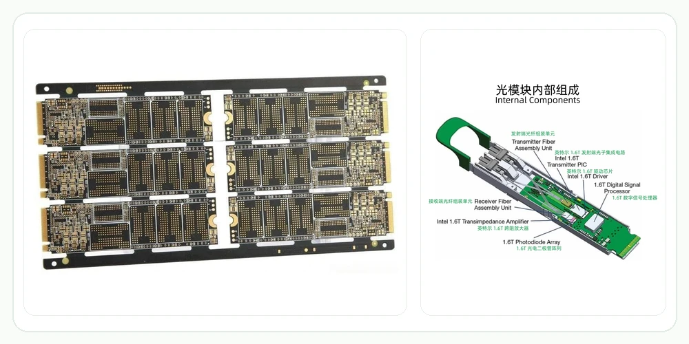
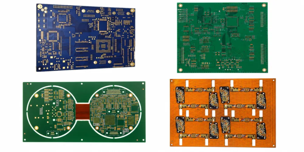
Optical module PCB panel and internal module component diagram
Optical Module PCB Dimensions, Surface Finishes and Mechanical Integration
A board that satisfies its stackup requirements must also meet the module’s physical assembly conditions. Highleap manufactures to the supplied outline, thickness and local dimension requirements, including card-edge or board-to-board interfaces where specified. These requirements become particularly important when the board must align with a compact housing, connector datum, thermal interface and high-density component placement.
Where the electrical host interface uses a plated contact edge, the drawing should identify the selective wear-contact finish, thickness and geometry. Hard-gold connector contacts and ENIG solder pads are different manufacturing features and may require separate process steps. The quotation should cover the actual combination of finishes, not assume a single gold process across the board. Fine-pitch component pads may also impose special via treatment, solder-mask opening requirements or finished surface flatness that affect both fabrication and assembly acceptance.
Thermal concerns must be translated into manufacturable features: copper distribution, thermal-via arrays, allowed board thickness, local contact surfaces and mechanical clearances. A supplier cannot certify the complete optical module’s cooling performance from a PCB fabrication drawing alone. But Highleap can manufacture the specified PCB features and coordinate them with the approved assembly drawing where both services are ordered.
If the housing limits edge thickness, bow and twist, or local coplanarity, those dimensions should be called out explicitly. Generic PCB dimensional tolerances may not cover a particular optical-module interface. The required measurement method, inspection frequency and reporting should be agreed as part of production acceptance, avoiding disputes after units are assembled into housings.
Compact Package Fit and Contact Processing
High-speed optical-module PCBs may have strict package-to-board interface constraints, including fine-pitch contacts, thin sections, narrow assembly keep-outs or controlled board flatness. Highleap reviews the actual mechanical datum drawing, not just nominal finished dimensions. Selectively plated hard-gold edge contacts, when specified, require a different process definition from ENIG on solder pads. Their plating area, thickness, edge bevel and measurement needs must be included in the original RFQ.
Finished thickness and bow/twist are examined with assembly support in mind. A PCB may satisfy its nominal stackup but still have excessive local distortion for a small fine-pitch package or module enclosure. If the client identifies critical components or mating features, the production acceptance plan can focus measurement on those dimensions, with an agreed sampling method rather than a generic appearance check.
Thermal Features Versus Electrical Performance
Copper pours and thermal-via fields can help transfer heat from active devices, but they interact with high-speed reference planes and package escape patterns. When the customer’s released design calls for copper coins, mixed copper weights or unusual cutouts, those special processes must be reviewed for manufacturability and quoted separately. Highleap can assess whether such a construction is compatible with the chosen substrate and stackup, but a thermal feature is not automatically included simply because the project is called an optical module PCB.
Manufacturing Verification and Repeat-Production Quality
For optical-module boards, quality is defined by the accepted production specification—not by the number of tests listed in a marketing description. Highleap’s manufacturing route can include inner-layer inspection, AOI, plated-hole integrity checks, finished-board electrical testing and customer-specified measurements. Where required, impedance coupons, microsections, material records or critical dimension reports are prepared according to the agreed inspection plan.
A first-article or qualification build should establish the approved combination of laminate, foil, stackup, plating, via processing, solder mask, surface finish and board outline. Once the customer’s program is released, production changes must be assessed for impact. Altering the laminate grade, foil profile, bonding sequence or copper thickness without approval can invalidate the assumptions behind previously accepted electrical results.
Highleap works from controlled file revisions and agreed fabrication notes for recurring orders. We can discuss material stocking, multiple release quantities, forecast schedules and delivery packaging as part of the commercial plan. For specialist low-loss materials, early demand visibility is useful because material procurement and qualification may be more significant constraints than the nominal PCB drilling or etching time.
When PCBA is included, the production acceptance plan should separate bare-board fabrication verification from SMT workmanship and any additional electrical testing. Our optical transceiver PCB assembly service can be quoted for customer-defined populated boards. Full optical module alignment, optical measurements and BER qualification are separate project requirements, not included merely because the PCB is used in an optical module.
From First-Article Approval to Repeat Lots
Prototype approval establishes that a particular combination of material, copper, drill, registration and finish processes can meet the customer’s drawing. Depending on the specified program, Highleap’s inspection package may include inner-layer AOI, final electrical test, dimensional checks, cross-section measurements and impedance coupon results. The method, sample size and acceptance criteria should be agreed in the purchase package. Bare-board evidence does not by itself certify a completed optical module’s eye diagram, bit-error rate or optical power.
On repeat builds, the approved stackup and revision remain the reference. If copper foil, laminate or prepreg becomes unavailable, the substitution is raised for review before it is incorporated. Changes that alter the channel or package interface should not be hidden inside purchasing notes. Lot identification, material traceability and delivery documentation can be scoped according to the OEM’s quality program; not every board requires the same reports, so Highleap quotes the actual requested evidence.
Cost and Lead-Time Variables That Affect Production Continuity
A high-speed module PCB may need an early reservation of specified low-loss material. Manufacturing quotations should therefore distinguish material lead time from factory processing time. Sequential build-up, backdrilling, microvia fill and selective plating can introduce steps that do not compress linearly on a rush order. For a forecast-driven product, agreeing on quantity breaks and allowable alternates helps stabilize availability without weakening the customer’s controlled specification.
Request a Custom Optical Module PCB Manufacturing Quote
To obtain a manufacturing quotation, provide the latest Gerber X2, ODB++ or approved equivalent files, NC drill data, layer stackup and material schedule, finished thickness, copper weights, special via notes and controlled-impedance table. Include the module or carrier outline drawing with critical dimension and surface-finish requirements. If a particular laminate, foil or bonding system is mandatory, identify it by grade and state the rules for substitutions.
Production-Ready RFQ Sequence
- Release the approved laminate and dielectric schedule, copper profile and impedance requirements.
- Supply layer maps for laser vias, filled pads, backdrilling and any other special interconnections.
- Define manufacturing acceptance reports, sampling and expected pilot-to-volume demand.
- Submit any alternates for explicit qualification rather than treating them as automatic substitutes.
For quote comparison and program planning, specify prototype quantity, pilot quantity, estimated recurring volume, required inspection evidence, revision status and target shipment date. Flag nonstandard processing such as sequential build-up, resin-filled and capped vias, selective plating, special slots, backdrilling and dimensional tolerances. Where the order includes PCBA, add the BOM, placement data, assembly drawing, sourcing responsibilities and approved test coverage.
Highleap Electronics can review the complete manufacturing package, identify process or material questions, and provide a quotation based on the agreed bare-board or assembled-board scope. Request optical module PCB fabrication and assembly pricing with your project specifications. The resulting quote is tied to the actual manufacturing route and deliverables, rather than a generic price attached to a data-rate label.
Quote Against a Controlled Platform Revision
The production inquiry should include material brand and exact grade where fixed, stackup and target finished thickness, copper and dielectric requirements, channel/impedance specifications, the interconnect map, and all drilling, fill, capping and backdrill notes. Mechanical details such as gold-contact boundaries, mounting positions, keep-outs and critical finished dimensions should be tied to the same PCB revision. If a test coupon or compliance report is required, include the method and acceptance limit rather than a general request for “high-speed testing.”
If Highleap is to supply assembled boards, provide the released BOM and approved alternatives, assembly files, component handling requirements and board-level test specification. The final quotation can then identify distinct fabrication, components, assembly and inspection charges. For 400G, 800G and 1.6T programs with multiple revisions, label each RFQ with the specific project and design revision so estimates and production records remain comparable.
OPTICAL MODULE PCB FABRICATION
Planning an Optical Module PCB Build?
Send your released stackup, material requirements, via map and volume target for production review.
Pricing, process and schedule are confirmed after engineering review.

Recommended Posts
Precision Press Fit PCB Manufacturing with Tight Tolerances
Press-fit PCB manufacturing requires close coordination...
8 Layer HDI PCB Manufacturer in China
Highleap Electronics provides 8 layer HDI PCB...
8 Layer Rigid-Flex PCB Manufacturing and Cost Guide
An 8 layer rigid-flex PCB combines multilayer rigid...
8 Layer PCB Cost in China: Rigid, Flexible & Rigid-Flex Pricing
How much does an 8 layer PCB cost? The answer depends on...
How to get a quote for PCBs
Let‘s run DFM/DFA analysis for you and get back to you with a report. You can upload your files securely through our website. We require the following information in order to give you a quote:
-
- Gerber, ODB++, or .pcb, spec.
- BOM list if you require assembly
- Quantity
- Turn time
In addition to PCB manufacturing, we offer a comprehensive range of electronic services, including PCB design, PCBA, and turnkey solutions. Whether you need help with prototyping, design verification, component sourcing, or mass production, we provide end-to-end support to ensure your project’s success.
For PCBA services, please provide your BOM (Bill of Materials) and any specific assembly instructions. We also offer DFM/DFA analysis to optimize your designs for manufacturability and assembly, ensuring a smooth production process.