
Optical Communication PCB Manufacturer for Fiber Network Equipment
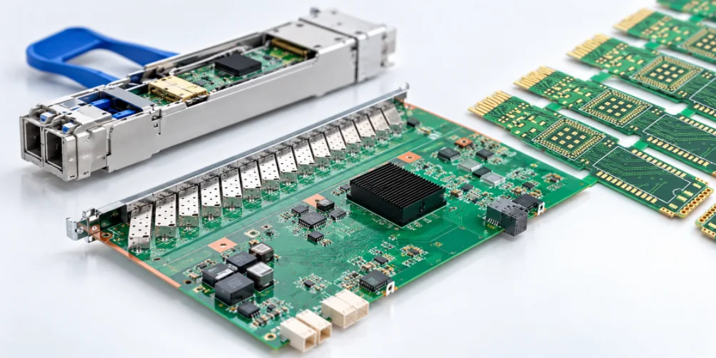
Highleap Electronics manufactures and assembles optical communication PCBs for fiber-network equipment, optical transport systems, telecom infrastructure and high-speed network hardware. Our services cover customer-designed multilayer, high-speed and HDI bare boards, as well as SMT and through-hole PCB assembly where the project requires populated circuit boards. We produce to released fabrication and assembly files, with materials, dimensions, test requirements and delivery quantities defined in the purchase specification.
Optical communication equipment uses several distinct PCB categories. A switch or optical-transport host board, an interface line card and a board inside a pluggable optical module do not carry the same mechanical, interconnect or test requirements. Highleap supports these projects with a fabrication review based on the actual board type, then coordinates a manufacturing route suited to its size, stackup, connector density and inspection scope.
Our focus is dependable PCB and PCBA supply for equipment manufacturers. Send the released Gerber/ODB++ data, stackup, connector drawings, assembly documentation where needed and expected production quantities for a commercial and engineering review.
Table of contents
- Optical Communication PCB Supply for Network Equipment Manufacturers
- Multilayer and High-Speed PCB Fabrication for Optical Network Hardware
- Optical Port Interfaces, Connector Geometry and Mechanical Acceptance
- PCB Assembly for Optical Communication Equipment
- Inspection, Traceability and Supply for Production Programs
- Request an Optical Communication PCB Fabrication and PCBA Quote
OPTICAL COMMUNICATION EQUIPMENT PCB
Need PCB Fabrication or PCBA for Network Hardware?
Share your board drawings, connector specifications, quantities and assembly scope for an equipment-board quotation.
Request an Optical Communication PCB Quote →Optical Communication PCB Supply for Network Equipment Manufacturers
Highleap serves customers building optical-network infrastructure and electronic equipment that connects, switches, transports or manages fiber-based communications. The PCB supply scope may include a dense network processing board, an optical transceiver host interface card, an optical transport or line card, or a compact control and power board assembled into the larger system. We quote the actual circuit-board design, not an assumed standard PCB implied by the industry name.
| Board in the equipment | Typical fabrication requirements | Important assembly or integration concern |
|---|---|---|
| Optical transport / line card | Multilayer stackup, high-density connectors, controlled impedance | Board stiffness, connector position, service access and test strategy |
| Network switch or host-interface PCB | High-speed copper channels, differential impedance, backdrill where specified | Pluggable-module cage footprint, host connector alignment, thermal and power components |
| Optical access / network control board | Mixed control, power and communications circuitry, multilayer routing | Connector durability, programming, board-level function checks |
| Custom optical communications subassembly | Application-defined outline, material system and special interfaces | Project-specific component sourcing, inspection and shipment configuration |
A full system procurement program may involve more than one board revision or construction type. Highleap can review a bill of boards or staged release schedule, with each design retaining its own stackup, acceptance criteria and quoted quantities. Customers seeking the small board inside the pluggable module, rather than the equipment host board, can use our dedicated optical transceiver PCB manufacturing service for that separate product family.
Highleap also provides PCB manufacturing for other telecommunications applications. For optical-network equipment, the fabrication and assembly scope is reviewed against the actual host-board or line-card requirements.
Board Families Included in an Equipment-Level RFQ
Highleap manufactures and assembles printed circuit boards for optical communication equipment programs, including host-interface cards, optical port interface boards, switching and aggregation hardware, control boards and equipment-level power or management PCBs. These are not all equivalent products. A host board populated with high-density pluggable cages, for example, has very different connector, thickness and mechanical requirements from a compact optical-module PCB. We quote the customer drawing and service scope for the specific board type, even where several board families belong to one equipment platform.
When an OEM purchases several boards for the same rack or chassis, Highleap can review them under a coordinated production program while retaining separate stackups, acceptance criteria and BOMs. A signal backplane may have press-fit connector requirements, a line card may require low-loss material and controlled via stubs, and a power board may require thick copper and high-current isolation. Treating them as one generic “optical communication PCB” risks omitting the processing differences that drive cost and yield.
Production Scope for Network Equipment OEMs
The manufacturing scope can cover bare boards, populated PCBAs or a defined mix of both. A system supplier may want only the high-speed bare line cards but need turnkey assembly on auxiliary controls. Highleap identifies which drawings, inspection records, fixtures and components apply to each deliverable. Equipment integration, chassis acceptance and optical-system performance testing are separate unless they are expressly included in an agreed project. This allows procurement to consolidate suppliers without blurring where bare-board, PCBA and final-equipment responsibilities begin and end.
Multilayer and High-Speed PCB Fabrication for Optical Network Hardware
Highleap Electronics manufactures high-speed multilayer PCBs for optical network hosts, switch line cards, transport equipment and related electronic assemblies. These designs can combine large board outlines, dense connector arrays, multiple power domains and long controlled-impedance routes. Manufacturing success depends on a repeatable stackup, registration and drilled interconnect quality—not simply a high layer-count claim.
For network-equipment boards, an isolated minimum-feature number is rarely enough to qualify the build. Total panel size, laminate grade, copper weights, hole count, connector locations, via structure, testing requirements and shipment format interact. A production proposal is reviewed against the complete fabrication package so material procurement, panelization and inspection can be planned for stable repeat orders.
Key Fabrication Controls for Optical Communication Equipment PCBs
-
Large-panel dimensional and registration control: Oversized host boards and line cards may require careful panel selection, artwork registration and handling through lamination, drilling and routing. Highleap checks finished outline dimensions and critical mechanical datums against the proposed manufacturing panel. Where an equipment chassis or card guide sets a tight tolerance, the customer drawing must identify its actual measurement conditions rather than leaving acceptance to a general board-size tolerance.
-
Controlled dielectric and copper construction: High-speed lines must be fabricated against the specified core/prepreg schedule, copper profile and final plating conditions. A change in laminate grade or dielectric thickness can affect controlled impedance and the validated channel. For hybrid material arrangements, compatibility and bonding details are assessed before release; a less expensive substitute is not adopted without authorization.
-
Through-via and backdrill strategy: Equipment PCBs can have long plated through-hole connections whose remaining stubs may matter for particular channels. The approved drill drawing defines layers, hole diameters and any requested backdrill depth or residual-stub limit. Not every host PCB requires backdrilling, and a fabrication supplier should not assign a generic stub target without the customer’s channel specification and verification method.
-
Power distribution and mixed copper requirements: Network boards may carry power planes, grounding structures and tightly routed digital signals on different layers. Mixed copper weights or locally high current can affect etching allowances, drilling, plating and finished thickness. The cost impact is reviewed at the full board level to avoid treating a heavy-copper requirement as if it applied equally to every signal layer.
-
Connector-dense fabrication clearances: Press-fit arrays, fine-pitch surface-mounted connectors, shielding contacts and mounting holes impose different dimensional and metallization requirements. Hole-to-copper spacing, annular rings, board-edge clearance and connector-specific hole tolerances must be assessed as a combined assembly interface. A board passing a basic electrical test may still fail a critical chassis or connector fit check.
-
Panel yield and production acceptance: Large boards consume more panel area, and a single rejected panel can have a significant material impact. Highleap evaluates process difficulty and defined inspection points to limit late-stage scrap. The approved acceptance package can include dimensional inspection, electrical testing, impedance coupons or traceability records as required; their scope should be confirmed before pricing.
Production Review for Network-Equipment OEMs
Related options are described in Highleap’s high-speed communication PCB fabrication service. For a repeat production program, the build is controlled by the released board revision, critical connector dimensions, accepted materials and inspection plan. This helps avoid a price based on an unrealistically simple construction and reduces surprises during pilot-to-volume transfer.
Optical Port Interfaces, Connector Geometry and Mechanical Acceptance
Optical communication equipment often includes host-side PCB connectors, transceiver cages, backplane interfaces and board-to-board interconnections. Highleap manufactures the host boards and related electronics against customer-specified connector and mechanical drawings. The host PCB is not the small PCB inside a pluggable optical transceiver: its responsibilities include chassis-level routing, connector mounting, power distribution and system assembly alignment.
Errors at this interface may only appear when the completed PCB is installed into a cage, faceplate or system enclosure. A connector part number, footprint data and mounting datum therefore need to match the fabrication files. Where the interface relies on press-fit compliant pins, the finished plated-hole diameter and plating conditions must follow the connector manufacturer’s application specification and approved assembly process—not a generic drilled-hole size.
Connector and Port Features Requiring Manufacturing Control
-
Pluggable cage and host connector alignment: Board outline, connector lands, mounting holes and faceplate datums should be assessed as one mechanical chain. If the PCB is fabricated within a nominal outline tolerance but its mounting features are displaced relative to the port opening, assembly may still fail. Critical relative dimensions and inspection positions need to be identified in the released drawing.
-
Press-fit finished holes: Press-fit pin compatibility depends on the connector-approved finished-hole range, plating condition, hole position and board support during insertion. The drill-tool diameter is not the finished plated-hole diameter. A board made using ordinary through-hole tolerances should not be assumed compatible with a press-fit connector unless the required interface specification has been reviewed.
-
High-speed host-side routing and returns: Fine-pitch connector breakouts can place sensitive differential pairs beside power and control pins. The PCB supplier manufactures to the approved reference-plane and impedance geometry, including specified layer transitions and via treatments. The design’s signal-integrity owner remains responsible for the electrical targets; fabrication changes that affect controlled geometry require approval.
-
Shielding, grounding and board-edge features: Cage grounds, shield-contact locations, mounting clearances, plated or non-plated slots and keep-out regions require their own documented finish and tolerance requirements. Selective edge metallization or a specialized slot process should appear explicitly in the RFQ rather than being inferred from a connector drawing that has not been reviewed by the fabrication engineer.
-
Tall connectors and PCBA mechanical handling: Large backplane and optical-port connectors can constrain SMT sequence, tooling access and reflow or subsequent assembly operations. Fabrication and assembly teams coordinate board flatness, panel rails, component keep-outs and support-fixture locations when both services are ordered. Connector insertion equipment and any special post-insertion test are included only when separately confirmed in the project scope.
-
Fit inspection and release control: Dimensional verification may need to use chassis or connector datums rather than arbitrary board corners. A bare-board E-test cannot prove connector seating or faceplate alignment. If assembly reveals a mismatch, Highleap and the customer review the PCB revision, connector drawing, assembly fixture and inspection records before any unauthorized correction or rework.
Keep the Host-Board and Module-Board Workscopes Separate
A customer sourcing the circuitry inside a pluggable module can refer to our custom optical transceiver PCB offering. The present equipment-board service addresses the larger host hardware and its assembly interfaces. Keeping their drawing packages, acceptance criteria and BOM boundaries separate supports more accurate quotations and avoids treating two different products as interchangeable.
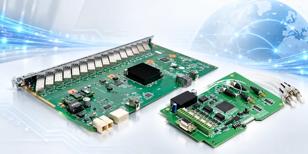
Optical communication PCB assemblies with network and fiber interfaces
PCB Assembly for Optical Communication Equipment
Highleap provides PCB assembly for customer-designed optical communication hardware, including component sourcing, SMT production, through-hole assembly where required, and defined inspection/test operations. A combined bare-board plus PCBA order can reduce the handoff risk between fabrication and SMT when the design uses dense connectors, fine-pitch ICs, large BGAs or mixed high-current and high-speed circuitry.
For an equipment host board, the BOM may include devices with allocation or lifecycle issues that need to be addressed before a build is scheduled. Our sourcing review uses manufacturer part numbers, approved alternates, demand quantity and customer restrictions. Components that require special handling, high-temperature exposure limits or process qualification should be identified before material purchasing and line setup.
Assembly planning also reviews board size and panel support, solder-paste access near connector fields, thermal mass differences, stencil strategy and inspection access. A large line card may require different support and handling arrangements from a compact interface daughterboard even if both contain similar component packages. Where the design needs programming, boundary-scan, functional testing or system-level interface checks, the required fixture, firmware, test instructions and pass/fail limits should be supplied or specifically agreed.
The communication PCB assembly service provides a related general assembly scope. For the special case of populated boards inside optical transceiver modules, our optical transceiver PCB assembly page describes that different PCBA requirement.
PCB-to-PCBA Process Coordination
For a line card or interface board, the bare PCB must be ready for the chosen assembly process. Connector solderability, the location of heavy components, board support during reflow and inspection access should be evaluated while the panel is being defined. Highleap can coordinate fabrication and SMT/THT assembly under the same revision-control workflow. This is particularly useful when the project has large connectors, heat sinks, shielding or press-fit features that need specialized insertion or support fixtures.
The assembly RFQ identifies which items are supplied by the customer and which are sourced by Highleap. For expensive or long-lead network ICs, the supply plan should include approved part numbers, alternative sourcing policy, moisture handling and traceability needs. The production plan also considers whether through-hole or press-fit connectors are installed before or after SMT operations; sequence changes can affect fixture access and soldering quality.
Testing Responsibility for Populated Communication Boards
AOI and X-ray inspection can help assess component placement and hidden solder joints, but they do not by themselves establish the operation of a multiport optical switch line card. Highleap quotes board-level electrical and functional testing against an agreed procedure, fixture and acceptance limits. System software integration, optical link qualification and fully populated chassis testing require their own explicit work scope. Separating these levels prevents a general “tested PCBA” phrase from hiding a gap between supplier and OEM responsibility.
Inspection, Traceability and Supply for Production Programs
Highleap’s fabrication and assembly services can be organized around the customer’s production acceptance plan. Bare-board work may include AOI, electrical testing, drilling and plating verification, dimensional checks and customer-requested controlled-impedance reports. PCBA inspection can include solder-paste and placement controls, AOI, appropriate X-ray inspection for hidden joints, and agreed electrical or functional tests. The delivered documentation and lot coverage are defined by the purchase and quality requirements, not presumed to be identical for every network board.
For network hardware intended for continuous service, consistency across repeat orders is a commercial requirement. Material grade, stackup, copper construction, connector geometry, approved component substitutions and firmware revision should remain traceable to the released manufacturing package. We can discuss first-article requirements, serialized or lot-based labeling, packing requirements and scheduled release plans with the customer before quoting recurring production.
Inspection evidence should not be overstated. Bare-board electrical testing verifies continuity and isolation under its approved test method; it does not by itself certify system signal margin or interoperability in an optical network. Likewise, SMT inspection supports soldering quality but does not replace a customer-defined board functional test or network-system qualification. These boundaries are documented so the buyer receives the agreed verification rather than a vague promise of “100% tested” without a test definition.
When a program is transferred from another supplier, we recommend releasing the same controlled board data, critical inspection characteristics and approved material/finish notes used in the accepted design. Differences between drawing revisions and previous production assumptions should be resolved in engineering review, before they become delivery interruptions.
Production Records for Long-Lifecycle Network Products
Optical network equipment may be produced in recurring batches over an extended program life. Highleap manages each build against released design files and ordering requirements. The customer’s qualification package may call for controlled material grades, IPC acceptance criteria, test coupons, lot identification, dimensional measurements or specific documentation. The quote should identify which records are standard and which are project-specific so manufacturing and procurement have the same acceptance baseline.
A component obsolescence event or late board revision can affect several boards in an equipment family. Separate revision identifiers for each assembly help prevent mixed builds and mistaken substitutions. Engineering changes that affect connector footprints, layer stackups or plating requirements are reviewed before the next order. When customers require traceable component lots or special packaging, those deliverables should be agreed at the outset rather than assumed.
Forecast, Inventory and Delivery Planning
The price of a large multilayer board is affected by material commitments, panel efficiency, yield and the size of the production batch. A one-time prototype price is not a reliable measure of future recurring cost. For annual programs, Highleap can quote specified quantity breaks and discuss the required delivery schedule based on material availability and approved alternates. Where a long-lead laminate or connector is prescribed, the lead time must include its procurement constraints, not simply the nominal factory processing days.
Request an Optical Communication PCB Fabrication and PCBA Quote
For bare-board pricing, provide the latest Gerber X2 or ODB++ files, NC drill data, board outline, stackup, laminate grades, controlled-impedance information, finished thickness, copper weights, surface finish and expected quantity. For host connectors or press-fit interfaces, include the connector part number, mechanical datum requirements, approved plated-hole specifications and any special inspection notes. State any mandatory material or component source restrictions.
Production-Ready RFQ Sequence
- Provide one controlled fabrication drawing package for each host PCB or line card.
- Add connector application documents, mechanical datums, press-fit requirements and system clearances.
- Define whether the RFQ includes bare boards, components, SMT/THT assembly or both.
- State scheduled quantities, inspection records, shipment form and any production-change controls.
For populated boards, add the BOM with approved alternates, centroid data, assembly drawing, programming and test requirements, component-sourcing responsibilities and any fixtures or mechanical assembly needed after soldering. Clarify whether the quote covers PCB fabrication only, a populated board, or a larger subassembly; optical link or complete equipment-level tests require a separately agreed scope.
Highleap Electronics can review the specified PCB construction and assembly requirements for prototype, pilot and production orders, then confirm open technical questions, scope, price and feasible lead time. Send your optical communication PCB manufacturing or assembly RFQ with your drawings and desired delivery quantities. Our quotation is based on the boards and acceptance requirements you actually need for your equipment program.
One RFQ Package Per Board, One Program View for the Equipment
For multiple optical communication boards, supply individual Gerber/ODB++ and drill sets, controlled stackups, mechanical drawings and order quantities for each part number. A master equipment BOM is not enough to release an individual PCBA: each board needs its own component BOM, placement data and revision. Where the same assembly has press-fit connectors, controlled-depth features or tight front-panel tolerances, include the corresponding application specifications. Highleap can review these packages together while retaining independent fabrication and acceptance scopes.
State whether the purchase is for bare PCBs, assembled line cards, auxiliary control boards or a combined order. Identify the tests that must be delivered with each assembly and the tests that the OEM will perform later. A complete scope lets Highleap prepare practical prototype and repeat-production quotations without treating all network boards as a single generic product.
OPTICAL COMMUNICATION EQUIPMENT PCB
Need PCB Fabrication or PCBA for Network Hardware?
Share your board drawings, connector specifications, quantities and assembly scope for an equipment-board quotation.
Pricing, process and schedule are confirmed after engineering review.

Recommended Posts
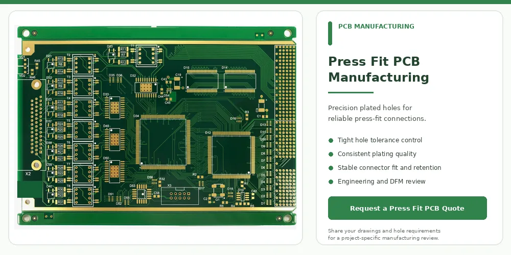
Precision Press Fit PCB Manufacturing with Tight Tolerances
Press-fit PCB manufacturing requires close coordination...
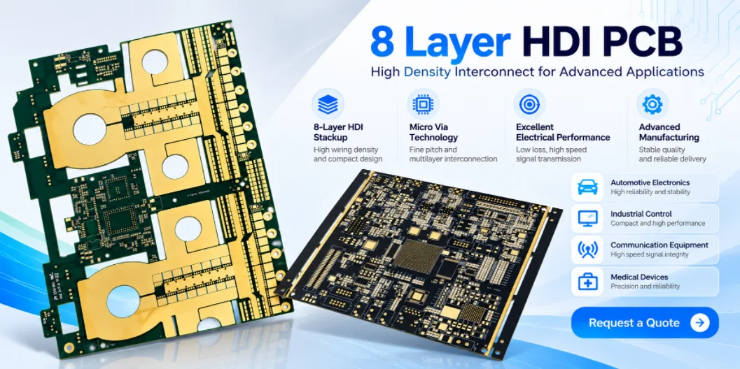
8 Layer HDI PCB Manufacturer in China
Highleap Electronics provides 8 layer HDI PCB...
8 Layer Rigid-Flex PCB Manufacturing and Cost Guide
An 8 layer rigid-flex PCB combines multilayer rigid...
8 Layer PCB Cost in China: Rigid, Flexible & Rigid-Flex Pricing
How much does an 8 layer PCB cost? The answer depends on...
How to get a quote for PCBs
Let‘s run DFM/DFA analysis for you and get back to you with a report. You can upload your files securely through our website. We require the following information in order to give you a quote:
-
- Gerber, ODB++, or .pcb, spec.
- BOM list if you require assembly
- Quantity
- Turn time
In addition to PCB manufacturing, we offer a comprehensive range of electronic services, including PCB design, PCBA, and turnkey solutions. Whether you need help with prototyping, design verification, component sourcing, or mass production, we provide end-to-end support to ensure your project’s success.
For PCBA services, please provide your BOM (Bill of Materials) and any specific assembly instructions. We also offer DFM/DFA analysis to optimize your designs for manufacturability and assembly, ensuring a smooth production process.