
VIPPO PCB Fabrication for BGA and Thermal Pad Designs
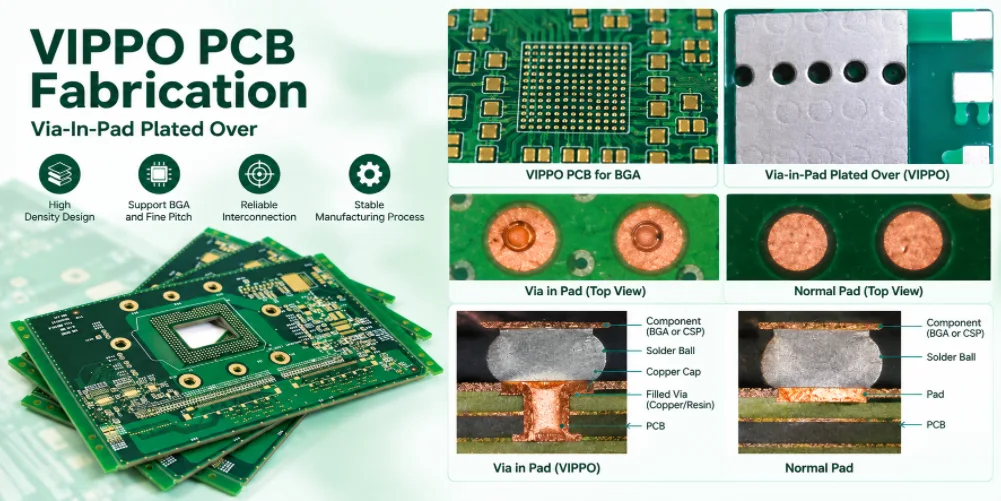
Highleap Electronics provides VIPPO PCB fabrication for designs that require via-in-pad structures with a defined fill and plated-over surface. VIPPO is often specified under fine-pitch BGA or LGA packages, exposed thermal pads and dense layouts where ordinary open or tented vias are not suitable. If your current PCB supplier cannot meet the via fill, cap or finished-pad requirements, send us the fabrication files for review.
A reliable VIPPO PCB manufacturing quote must define the via construction rather than rely on the phrase “via in pad” alone. Via diameter, pad geometry, fill type, copper cap, planarity, surface finish and inspection criteria all affect cost, lead time and assembly results. Highleap reviews these details with the intended application in mind so the quoted build matches the required structure.
Table of contents
- What Is VIPPO PCB Fabrication?
- VIPPO vs Open Via and Filled Via-in-Pad PCB Designs
- VIPPO PCB Manufacturing Process: Via Filling and Copper Capping
- VIPPO PCB Assembly and Soldering Requirements for BGA
- VIPPO PCB Design Guidelines for Fine-Pitch BGA
- VIPPO PCB Manufacturer for Filled and Plated-Over Vias
- VIPPO PCB Fabrication FAQs
VIPPO PCB
Need a VIPPO PCB Fabrication Quote?
Send the Gerber files, drill data, via-fill specification and BGA footprint details. Highleap can review the via-in-pad construction and required copper cap before quotation.
Request a VIPPO PCB Quote →VIPPO means Via-In-Pad Plated Over. Specify the fill material, cap quality, planarity and surface finish separately.
What Is VIPPO PCB Fabrication?
VIPPO stands for Via-In-Pad Plated Over. The via is located within a component pad, filled using the specified process, planarized as required, and plated over with copper to create a continuous pad surface. “Open” is not part of the acronym; it describes an opening or exposure condition and should be specified separately where relevant.
- Via-in-pad location: the via lies within the component land rather than beside it.
- Fill specification: the drawing or fabrication notes identify the required fill material and acceptance criteria; resin and conductive fills are not interchangeable.
- Plated-over surface: copper is deposited over the filled via to form a continuous, solderable surface. Planarity, cap integrity and surface finish should be defined for the application.
The reason the distinction matters is that several of these steps are optional in a standard board and each one that is added changes what the fabricator has to control. A via that is drilled and tented is essentially free. A VIPPO structure requires a controlled fill, planarization as needed, copper cap and surface-finish sequence. The solder-mask opening around the finished pad is specified separately; it should not be confused with an open or unfilled via. The material supplier may tell you “we do via in pad” and mean the filled-and-capped version, the tented version, or the resin-plugged version, so the terminology has to be pinned down in the artwork notes.
VIPPO vs Open Via and Filled Via-in-Pad PCB Designs
This is the distinction that most often causes a quote to move. Each row below is a different physical structure with a different thermal path, a different cost, and a different failure risk.
| Construction | Physical structure | Thermal behaviour | Cost and risk |
|---|---|---|---|
| Tented via | Normal plated barrel, covered by solder mask | Heat still conducts down the barrel, but the thermal path is broken at the pad surface | Lowest cost; the default when nothing is specified |
| Capped via | Via plated, then covered by a copper cap, pad still masked | Good; the cap restores a continuous copper surface | Adds a capping cycle; cap adhesion and coplanarity need control |
| Filled and capped via | Barrel plated, via filled with copper paste or resin, cap plated over the fill | Best; a solid copper column from surface to inner layer | Highest cost and longest route; fill shrinkage and cap adhesion are the risks |
| Resin plug via | Barrel plated, via filled with resin, surface left as resin | Poor as a heat path; the resin is an insulator | Used to seal the via for RF or cleanliness reasons, not for thermal reasons |
Only the third row is a true VIPPO. If a design says “via in pad, open” without specifying the fill, the fabricator may deliver any of the four. Our guide to via filling and copper plating covers the fill and cap processes in detail, and the differences between the resin and metal fill approaches are set out on our resin-plugged via construction.
Why Use Copper-Capped Via-in-Pad for BGA PCBs?
For a thermal pad, the goal is a predictable thermal path from the pad into the board’s copper structure. A properly filled and plated-over via provides a continuous surface for soldering and avoids the open-hole solder-wicking path associated with an unfilled via. Thermal performance still depends on the fill material, via array, connected copper layers and the surrounding stackup.
The same argument applies to RF. A via that is tented and sits in the middle of a ground plane region is a small patch of discontinuity; a via that is filled and plated over is continuous copper. In a design where a via is deliberately placed to break a plane or create a known stub, the reverse logic applies and the via should be open, not tented, so that the structure is defined rather than accidental.
Because the via is open, the surface finish becomes a functional requirement rather than a cosmetic one. ENIG is the usual choice for a via that will be soldered to, because it stays flat and solderable over a long shelf life. ENEPIG is used where the thermal performance of immersion silver is wanted together with a solderable surface. Immersion silver will tarnish in sulphur-bearing air, which matters if the boards sit in storage before assembly. Our surface finish selection for RF and microwave boards covers this trade-off, and the general options are compared in our ENIG surface finish process.
VIPPO PCB Manufacturing Process: Via Filling and Copper Capping
The sequence below explains why a VIPPO board is not simply a standard board with a note attached. Each step is a separate cycle with its own controls, and the order is not freely adjustable.
| Step | Process | What it has to achieve |
|---|---|---|
| Drilling | Mechanical or laser drilling to the specified diameter | A clean barrel wall. For laser drilling, the aspect ratio and the hole diameter determine which source is used |
| Deburr and desmear | Mechanical deburring plus chemical or plasma desmear | A wall that will accept plating and a fill material. Skipped or shortened on a resin plug, this is the origin of fill adhesion failures |
| Plating | Electroless copper seed followed by electroplating, with the barrel mask in place to protect the fill surface if a fill is used | Barrel copper at the required thickness. The barrel mask must survive the plating bath and the plating must be uniform inside the hole |
| Fill | Via filling by screen print or stencil for larger holes, or by lamination under vacuum for microvias and dense arrays | Avoid voids in the column. Voiding is the main cause of a VIPPO that fails to carry current or heat |
| Capping | Thin copper cap plated over the fill, or a separate copper foil laminated onto the fill | Continuous copper over the via, bonded to the fill and to the surrounding pad |
| Mask and finish | Solder mask applied with the VIPPO pads left open | Mask must not be left in the via, and must not peel off the cap. This is the most common defect on VIPPO boards |
Two details in that table decide whether the process works. The first is control of the fill and surface preparation before capping, which affects cap adhesion and planarity. The second is the solder-mask definition around the finished pad: the mask opening must match the package land pattern, and should not leave unwanted mask residue on the solderable surface. The relationship between fill, cap and mask is covered in more detail on our HDI PCB manufacturing.
Copper-Filled vs Resin-Filled VIPPO Vias
If the design calls for a filled, plated-over via, the fill material is a decision with real consequences. The two common choices are metal and resin, and they are not interchangeable.
- Copper paste fill produces a solid metal column. It conducts heat and current, and it can be plated over directly. It shrinks during sintering, so the hole must be slightly smaller than the target, and it requires a sintering profile that will not damage the laminate. This is the correct choice when the via has to carry heat or current into an inner layer.
- Resin fill seals the via and can provide a surface for subsequent planarization and capping. Resin is generally less thermally conductive than copper, so the thermal path must be assessed against the design target rather than assuming resin fill and copper fill perform alike.
Two further variants exist. Via fill by lamination uses a film of filler in the prepreg so that the fill is applied in the same press cycle as the lamination, which is the standard route for microvia structures in sequential builds. Selective fill fills only designated vias on a panel that contains both filled and unfilled via structures, which is how a board with thermal vias on one area and resin-sealed vias elsewhere is made. The trade-offs of the resin approach are described on our resin plug hole page, and the sequence-dependent nature of the process is set out in our sequential lamination for HDI PCBs.
HIGHLEAP ELECTRONICS · PROJECT INQUIRY
Request a VIPPO PCB Fabrication Quote
Highleap Electronics provides VIPPO PCB fabrication for defined via-in-pad fill and plated-over requirements. Send your drill data, stackup, pad geometry and acceptance criteria so the required construction can be quoted accurately.
Gerber / ODB++ + stackup + critical requirements.
VIPPO PCB Assembly and Soldering Requirements for BGA
Solder wicking is primarily a concern when solder can enter an open or incompletely capped via. A correctly filled and plated-over VIPPO pad is designed to provide a continuous solderable surface. Assembly risk can still arise from cap defects, excessive dishing, poor planarity, unsuitable pad geometry or an incorrect solder-paste volume, so the fabricator and assembler should agree the acceptance criteria before the first build.
There are three ways this is controlled, and they are used in combination:
- Defined pad and via geometry. Specify via diameter, pad size, pitch and the required copper cap so the finished pad supports the component footprint and solder-mask design.
- Stencil aperture reduction on the pad. The paste stencil for the exposed pad is reduced in area so that the initial solder volume is matched to what the joint needs, rather than the volume the pad area would suggest. This is an assembly-side control, and it has to be agreed with the assembler, not just with the fabricator.
- Fill, cap and planarity verification. The specified fill material, cap integrity and finished-surface planarity should be checked against the drawing. The best fill choice depends on electrical, thermal, mechanical and reliability requirements.
The design rules that make this work are set out in our RF PCB via design, and the assembly-side process is described in our PCB assembly process. When a design has both VIPPO and a demanding thermal environment, it is worth agreeing the stencil reduction and the via pattern with both the fabricator and the assembler before the first article, because the two sides have to be consistent.
Common VIPPO PCB Defects and Reliability Risks
These are the defects that a VIPPO build can pass visual inspection and still fail in service.
- Fill voids. A column with a void in the middle conducts less than the drawing implies and is invisible from the surface. Where thermal performance is the design driver, this is the defect that matters most, and it is why fill process control rather than fill appearance is the item to negotiate.
- Cap delamination. The cap bond separates from the fill, leaving a void at the most stressed point in the structure. This becomes visible as an open circuit after thermal cycling.
- Cap or surface defects. Dishing, voids, cap separation or solder-mask contamination on the finished pad can compromise solderability and planarity. Acceptance criteria should distinguish a fill defect from a surface-finish or assembly-process issue.
- Insufficient solder at the joint. This may result from stencil design, paste volume, pad geometry or assembly settings. For a correctly capped VIPPO pad, do not assume solder wicking is the cause without inspecting the finished via and solder joint.
- Bare copper exposure and corrosion. An open pad is bare copper with no mask protection. If the design has an open via and no surface finish specified, or a finish that is not solderable, the pad is a corrosion site.
Verifying plated hole integrity is covered in our interconnect stress testing (IST), and general plated-hole reliability considerations are on our PCB reliability page.
VIPPO PCB Design Guidelines for Fine-Pitch BGA
These are the rules that decide whether the board is manufacturable, and they should be fixed before the artwork is released rather than discovered during review.
| Rule | Commonly applied value | Reason |
|---|---|---|
| Keep vias out of the solder mask opening edge | A defined setback from the pad edge, so the via barrel is fully inside the pad | Prevents mask from bridging onto the via and prevents the barrel from being exposed at the pad edge |
| Minimum via diameter and spacing in a filled array | Typically 0.20–0.25 mm finished hole with 0.20–0.30 mm of space between barrels | Allows the fill material to flow and the plating solution to reach the barrel interior |
| Limit fill voiding on thermal vias | Void acceptance limit stated per design, verified on sectioned samples | Voiding reduces the intended thermal and electrical path |
| Specify the fill material | Copper paste, resin, or fill by lamination, stated explicitly | The two fill materials have different thermal, electrical and assembly behaviour |
| Specify the surface finish on open pads | Usually ENIG or ENEPIG for soldered open pads | An open pad is bare copper and will not solder reliably without a defined finish |
Where a via passes close to or through a buried or blind via structure, the interaction between the two processes has to be checked rather than assumed, and that is covered on our blind and buried via page. A general review of the artwork against standard rules is available through our PCB design for manufacturability (DFM) review.
VIPPO PCB Manufacturer for Filled and Plated-Over Vias
For projects searching for a VIPPO PCB manufacturer, Highleap can review the specified filled-and-capped via structure, the surrounding pad design and the inspection requirements. The quotation should make clear whether the requested construction uses resin fill, conductive fill or another approved route, and what finished-surface criteria apply. This is especially important for VIPPO PCB fabrication for BGA, where pad coplanarity and solder-volume control can affect assembly yield.
For an accurate filled and capped via-in-pad PCB quote, provide the drill file, via diameter, pitch, pad dimensions, layer connection, board stackup, surface finish, fill specification and any customer acceptance standard. If the board will be assembled, include the BOM, pick-and-place file and assembly drawing so the fabrication and assembly requirements can be reviewed together.
Highleap’s via filling and plating process information is relevant to the fill and cap discussion, while HDI PCB manufacturing is relevant when VIPPO is part of a dense microvia or build-up construction. For a turnkey build, discuss the board and assembly scope through our PCB assembly services team.
- Quote package: Gerber/ODB++ data, drill file, stackup, via/pad geometry, fill and cap specification, surface finish, quantity and inspection criteria.
VIPPO PCB Fabrication FAQs
Is VIPPO the same as via in pad?
No. “Via-in-pad” describes the location of the via. VIPPO means Via-In-Pad Plated Over and specifies a filled via with a plated-over surface. The fill material, cap requirements, solder-mask opening and surface finish should be defined separately on the fabrication drawing.
Can VIPPO be combined with blind and buried vias?
Yes, but the two processes interfere with each other and the sequence matters. A via that is filled by lamination has to be filled in a press cycle, and a blind via buried in the same laminate may need to be exposed and plated in a later cycle. Boards combining both exist, but they need a deliberate process route rather than a stack of independent notes.
Does VIPPO affect the impedance of the affected nets?
It can, and in most cases favourably for power and ground nets, because a filled and plated via behaves as a solid copper column rather than a plated tube with a dielectric core. On a controlled-impedance signal net, the filled via presents a different impedance to an unfilled one, so the via model in the simulation should reflect the finished construction.
Can the boards be assembled after VIPPO fabrication?
Yes. Properly fabricated VIPPO pads are intended to support component soldering directly on the plated-over surface. The assembler should still review pad geometry, stencil aperture, solder-paste volume and package thermal-pad recommendations, especially for large exposed pads or fine-pitch BGA packages.
How is VIPPO verified?
By cross-sectioning filled vias on sample units to check the fill and the cap, by continuity and thermal resistance measurement where the design depends on it, and by inspection of the exposed pad for mask residue. The sample plan and the measurement method should be agreed in the quotation rather than assumed.
VIPPO PCB FABRICATION · RFQ
Request a VIPPO PCB Fabrication Quote
Send the Gerber, drill file, via diameter and pitch, fill material, surface finish and the pad construction. We confirm the route and quote the build with the fill and plating steps included.
Fill material + surface finish + sample plan.

Recommended Posts
Prototype PCB Assembly: From Design Files to Tested Boards
Highleap Electronics builds prototype PCB assemblies for...
Hard Gold Finger PCB Manufacturing: Plating and Beveling
Hard gold finger PCB manufacturing is used when a circuit...
Small PCB Panelization: Array Design and Depaneling
Imagine a 26 × 18 mm circuit that must pass through...
PCB Panelization for Volume Production: Cost and Yield
A fabrication panel that holds more boards is not...
How to get a quote for PCBs
Let‘s run DFM/DFA analysis for you and get back to you with a report. You can upload your files securely through our website. We require the following information in order to give you a quote:
-
- Gerber, ODB++, or .pcb, spec.
- BOM list if you require assembly
- Quantity
- Turn time
In addition to PCB manufacturing, we offer a comprehensive range of electronic services, including PCB design, PCBA, and turnkey solutions. Whether you need help with prototyping, design verification, component sourcing, or mass production, we provide end-to-end support to ensure your project’s success.
For PCBA services, please provide your BOM (Bill of Materials) and any specific assembly instructions. We also offer DFM/DFA analysis to optimize your designs for manufacturability and assembly, ensuring a smooth production process.