
Cavity PCB Manufacturing for Precision Board Designs
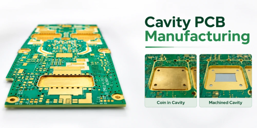
A cavity PCB is a purpose-built board with a recessed or locally machined region—not a standard PCB with an extra hole. Highleap Electronics provides cavity PCB manufacturing for designs that require component clearance, reduced local thickness, stepped pockets or defined cavity geometry. If your current supplier cannot support the required cavity depth, stackup or mechanical details, send us the fabrication package for a manufacturing review.
For a useful custom cavity PCB quote, our engineering review needs more than the Gerber outline. Cavity dimensions, depth reference, remaining material, wall geometry, nearby copper, laminate construction and any RF or mechanical function all affect the process route. We review these requirements before quotation so the price and lead-time discussion is based on the board you actually need.
Table of contents
CAVITY PCB
Need a Custom Cavity PCB Quote?
Send your Gerber files, stackup and a section view showing cavity depth and tolerances. Highleap will review the specified construction and advise on the manufacturing route.
Request a Cavity PCB Quote →Confirm the cavity opening, depth reference, remaining dielectric, copper clearances and wall finish on the fabrication drawing.
What Is Cavity PCB Manufacturing?
Start from a normal multilayer stackup and remove material from the core, either by milling a pocket from one side or by cutting a channel through the board with a router, then laminate skins back on top of what remains. The result is a board that is locally thinner than the rest of the panel, or hollow along a defined route.
What gets removed matters as much as what is left. If the pocket is milled in the core only and the prepreg skins stay bonded on top, the routing tool passes through the core and stops, which preserves a continuous outer surface for components and connectors. If the cavity is machined from the outside of a finished panel, the tool has to enter through a copper and prepreg layer, which is why the drawing usually has to state whether the cavity is open or closed and which layers terminate inside it.
Two consequences follow directly from this. First, any layer that terminates inside the cavity is a layer that must be routed around the pocket, so the artwork has to include the cavity outline as a keepout. Second, a milled pocket leaves copper edges at the pocket wall. If that wall is inside a ground plane region, the copper is no longer continuous there, and the design has to account for it rather than assume a solid reference plane.
Types of Cavity PCBs and Their Manufacturing Requirements
The term “cavity board” covers several distinct constructions. They are not interchangeable, and specifying the wrong one is the most common reason a cavity quote comes back much higher than expected.
| Cavity type | Construction | Typical purpose | Main risk |
|---|---|---|---|
| Core relief pocket | Material removed from the core only; prepreg skins remain | Reducing local thickness, creating a recess for a component or connector | Delamination if the pocket is not fully supported and skinned |
| Through cavity / channel | Router cuts a channel across the board; skins may be re-laminated over it | RF cavity, waveguide run, isolated cavity volume | Board rigidity loss and warpage after re-lamination |
| Blind pocket | Pocket milled from one surface, terminating inside the stackup | Cavity for an RF resonator or a mounted component | Copper termination inside the pocket must be defined on the drawing |
| Stepped cavity | Two or more pocket depths in one board | Locating components at different heights, hybrid RF and logic on one board | Two registration operations instead of one |
A blind pocket and a through cavity behave very differently in the artwork. The through cavity separates the board into regions that must be mechanically tied back together, usually by leaving material bridges or by re-laminating continuous skins. That is the structural decision that determines whether the part is feasible.
Cavity PCB Design Requirements for Board Strength and Depth
The laminate in a PCB is a fibre-reinforced composite, and its stiffness comes from the glass weave running through the core. Routing removes that reinforcement in the direction of the cut. A board with a wide, uninterrupted channel across it can flex under the loads of a bolted heat sink or a connector insertion force, and in a humid environment the reduced section also weakens the bond between the skins and the remaining core.
Three practices are common in this construction, and all three belong in the drawing rather than in the fabricator’s discretion:
- Material bridges: strips of core left in place across the cavity, so the cut does not run the full width. These are the standard method for keeping a cavity board from splitting into two pieces.
- Continuous skins: the outer prepreg layers are not interrupted, so the board retains a bending surface even where the core is removed. Where a cavity is open on both sides, an external skin has to be added afterwards, which changes the thickness at that point.
- Corner radii: an internal sharp corner in a routed pocket is a stress concentration and a delamination initiation site. Radius values are usually expressed in the drawing as a minimum radius rather than an exact dimension.
Rigidity can be checked before the build. If your board has a cavity and also mounts a heavy component, describe the mount method and the fastener torque in the RFQ, because the local bearing stress around the screw hole is often the limiting case rather than the board’s overall stiffness. This is where a mechanical drawing of the assembly, rather than only the PCB artwork, gives the fabricator what it needs. The same reasoning applies to the fastener and torque questions covered on our PCB mechanical design considerations page.
RF Cavity PCB Design for Ground Planes and High-Frequency Circuits
RF is where cavity construction earns most of its value, and also where it creates the subtlest failures. A milled cavity removes copper from the inner layers in the pocket region, which means the reference plane under that area is interrupted. For a cavity that forms part of a resonator, filter, or oscillator, that interruption is the point: the cavity dimensions set the resonant frequency, and the metal boundary defines the mode. For a cavity that is not intended to resonate, the same interruption still needs a defined boundary, or the structure will radiate and couple unpredictably.
Three parameters govern the result, and all three have to be stated:
- Cavity depth, which is the dielectric height of the resonant volume. Routing tolerance and skin thickness both eat into this, so the tolerance on depth needs to be tighter than the tolerance on the outer board thickness.
- Metal boundary definition: whether the cavity is defined by the remaining copper wall, by a plated slot, or by a separate metal part assembled into the pocket. These are not equivalent in RF terms.
- Dielectric material inside the cavity: the resin and filler in the core have different Dk and Df from the prepreg skins, so a cavity that spans both can shift the resonant frequency relative to a calculation based on a single material.
This is why cavity boards are normally specified alongside an RF material system rather than generic FR-4. Our RF and microwave PCB manufacturing guidance explains how stackup and material choices interact with impedance, and the material families themselves are compared on our microwave PCB materials. If the design is a cavity resonator rather than a general RF board, the material and the cavity tolerance are the two things worth getting agreed with the fabricator before artwork is released.
CAVITY REVIEW · BEFORE ARTWORK RELEASE
Confirm the Pocket, the Bridges and the Tolerance
Send the Gerber, stackup table and a section view showing the cavity depth and termination. We return a manufacturability answer on the specific geometry, not a generic quote.
Stackup table + section view required.
Cavity PCB Manufacturing Process and Inspection
A cavity board is not a standard build with an extra step. The routing has to be positioned relative to the layers that are already committed, and that constrains the whole sequence.
| Step | What happens | Where it goes wrong |
|---|---|---|
| Inner layers | Inner artwork imaged; the cavity outline becomes a keepout on the layers that terminate inside it | Copper drawn across the pocket that the designer intended to be absent |
| Prepreg and partial lamination | Skins bonded to the core; the cavity is still solid material | Core fill voids or resin flow into the region that will be routed out |
| Routing | Router mills the pocket or channel to the specified depth | Tool deflection on a wide pocket, glass fibre pull-out, copper burr at the wall |
| Skinning and second lamination | Outer skins applied over the routed region | Delamination where the pocket wall was not properly skinned, or air trapped in the pocket |
| Finish and test | Surface finish, then dimensional and electrical verification | Pocket depth measured after finish, which can differ from the routed depth |
The practical implication is that the cavity depth is a routed dimension sitting between two laminated surfaces, and it is measured after plating and finish. If a design needs a depth tolerance tighter than what routing and plating can hold, the answer is usually to move the cavity into a mechanical part rather than to ask the fabricator for a tighter cut. Cut tolerance questions are part of the file preparation covered in our PCB lamination process.
Cavity PCB vs Embedded Substrate: Key Differences
Both approaches put something inside the board, and they are often confused at the specification stage. They differ in what the board contains and in what the fabricator has to do.
| Aspect | Cavity construction | Embedded substrate construction |
|---|---|---|
| What is inside | Nothing, or a passive element placed into a machined recess | A complete circuit substrate, module or component carrier |
| Fabricator’s task | Route, skin and laminate around a volume | Prepare a recess, receive the substrate, bond and interconnect it |
| Interconnection to the host | Typically by component leads or by a separate interconnect | Defined pad-to-pad interface that must be designed before the substrate is made |
| Supply risk | Low; nothing exotic is inside | Higher; the substrate is a separate qualified part |
If the intent is to place an RF module or a small circuit inside the board, the embedded substrate route is usually the more controlled one, and it is covered in more detail on our embedded-substrate PCB construction. If the intent is to create an RF volume or to recess a discrete part, cavity construction is the right tool.
Cavity PCB Design Guidelines for DFM Review
These are the rules that most often force a redraw rather than a process tweak:
- Pocket wall distance to copper. Where the pocket wall terminates a plated via or a plane, the remaining annular material has to survive the second lamination cycle. A via too close to the pocket edge will be exposed on the wall and will not be covered by plating the way a normal via is.
- Support under the pocket floor. If the pocket is milled in the core and the cavity floor is left unsupported over a wide area, it will collapse or delaminate during the second press cycle.
- Registration between the routing step and the artwork. The pocket position must be tied to the artwork by the fabricator’s own process, and the tolerance has to be stated relative to features that matter, such as a via array or a connector footprint.
- Tool access and panelisation. The router has to reach the pocket. A pocket close to the panel edge, or a board that must be routed before or after panelisation, changes the panel layout. Our PCB panelization covers how panel strategies affect routing steps and where fixtures must be placed.
- Coplanarity at the skin. If components sit over the pocket, the surface has to stay flat within the component’s own tolerance, which limits how thin the skin may be and how much the panel can move between cycles.
The majority of these are ordinary DFM considerations applied to an unusual geometry. Our PCB design for manufacturability (DFM) review covers the standard rule set, and a cavity build is worth running through it in full because the routing step interacts with several of the normal rules at once.
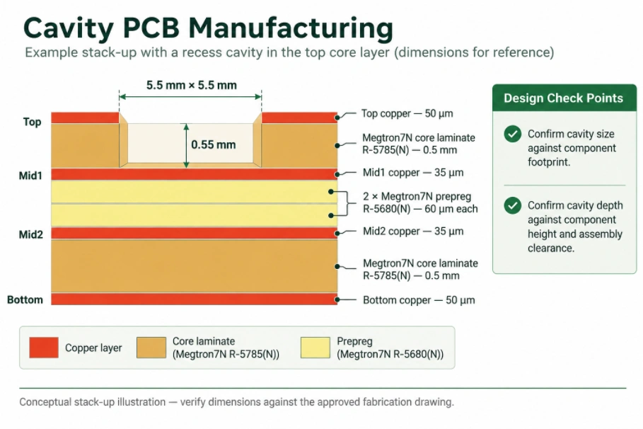
Cavity PCB Quote Requirements: Depth, Size and Tolerances
Most of the cost surprises on a cavity board come from information that was never on the drawing. The following list covers what a fabricator needs in order to price the build without guessing:
- Stackup with cavity position. Layer names, material, copper and prepreg thickness, and a clear statement of which layer the pocket is milled from and how deep it goes, measured from a stated reference surface.
- A section view through the cavity. This single view resolves more ambiguity than a page of notes. It should show the pocket floor, the skins above it, and any copper that terminates on the wall.
- Tolerance on cavity depth, and whether it is a bilateral or total-indication requirement.
- Wall treatment. Whether the pocket wall is left as bare laminate, plated, or covered by a separate metal part. This changes both the RF behaviour and the corrosion protection.
- Bridge and support details, or explicit permission to have the fabricator propose them based on its own tooling.
- Material system, especially if the cavity is part of an RF structure, where the Dk and Df of the core and prepreg both enter the calculation.
- Mechanical load. If any part of the assembly loads the pocket region, state the fastener torque and the load case.
- Acceptance criteria. What the cavity must be measured against, and whether the check is by sectioning, by coordinate measurement, or by an RF test on the finished board.
Stackup documentation conventions and how they should be written are covered in our PCB stackup design, and the laminate side of the question in our laminate construction overview.
Cavity PCB Manufacturer for Prototypes and Production
Highleap can support custom cavity PCB fabrication projects where the cavity geometry and material stackup can be matched to an agreed manufacturing route. We review cavity PCB prototypes as well as production enquiries, with the required inspection scope defined before release. The objective is to identify the critical dimensions and process assumptions early—not to quote a generic pocket operation that may not meet the finished-board requirement.
When requesting a cavity PCB manufacturing quote, include the finished board thickness, cavity length and width, depth tolerance, corner radius, cavity location, exposed-layer requirements and quantity. For RF cavity PCB designs, identify the ground-plane keep-outs, metal boundary and any controlled depth or electrical requirements. For component-clearance cavities, include the component outline and mechanical assembly drawing.
Highleap can also review the wider board build through our PCB fabrication services, while projects that combine cavity features with demanding RF stackups may also need a review of our high-frequency PCB manufacturing options. Submit your files through the PCB quote request and identify the cavity features that are critical to function.
- Quote package: Gerber or ODB++ files, drill files, stackup, dimensioned cavity drawing, depth tolerance, quantity and required inspection records.
Cavity PCB Manufacturing FAQs
Can a cavity board be assembled like a normal board?
Yes, if the skins over the cavity are continuous and flat enough for the assembly process. If the cavity is open on the top surface, the region needs mechanical support from the enclosure or a separate cover, and the assembly drawing has to say so. Standard SMT is fine on the skins; a cavity that interrupts the top copper surface limits where components can be placed.
Does routing the cavity affect the electrical performance of the other layers?
It can. Copper that is cut through at the pocket wall is no longer a continuous current path, and any layer running above or below the pocket sees a changed dielectric environment. The electrical impact depends on the affected layer geometry, return-current path, signal frequency and cavity boundary. RF and high-speed designs should evaluate the cavity in the electrical model rather than assuming the feature is purely mechanical.
What is the usual lead time impact?
A cavity build adds a routing operation, a second lamination cycle and additional inspection at each stage, so it is normally quoted as longer than the equivalent board without cavities. The added time depends more on the number of lamination cycles and the panel arrangement than on the size of the pocket. If the schedule is fixed, say so in the RFQ, because the process route can sometimes be arranged around it.
Can you build a cavity board with buried or blind vias?
Yes. The constraint is that vias have to stay clear of the pocket wall by enough distance to remain plated and covered after the second lamination cycle, and any via intended to terminate inside the cavity has to be defined explicitly rather than left to interpretation.
How is cavity depth verified?
By measurement of the finished board, typically by coordinate measurement of the pocket floor relative to the reference surface, and on a sample basis by cross-sectioning. If the depth tolerance is critical to your RF performance, ask for the measurement method and the sample plan in the quotation rather than assuming it.
CAVITY PCB MANUFACTURING · RFQ
Request a Cavity PCB Manufacturing Quote
Send the Gerber, stackup table, cavity depth and tolerance, wall treatment and any mechanical load data. We review the geometry and confirm the build route before you commit.
Stackup table + section view + tolerances.

Recommended Posts
Small-Batch High-Mix PCB Assembly for Repeat Orders
Highleap Electronics provides small-batch, high-mix PCB...

EVT DVT and PVT PCB Assembly: From Validation to Production
Highleap Electronics supports EVT, DVT and PVT PCB...
Prototype PCB Assembly: From Design Files to Tested Boards
Highleap Electronics builds prototype PCB assemblies for...
Hard Gold Finger PCB Manufacturing: Plating and Beveling
Hard gold finger PCB manufacturing is used when a circuit...
How to get a quote for PCBs
Let‘s run DFM/DFA analysis for you and get back to you with a report. You can upload your files securely through our website. We require the following information in order to give you a quote:
-
- Gerber, ODB++, or .pcb, spec.
- BOM list if you require assembly
- Quantity
- Turn time
In addition to PCB manufacturing, we offer a comprehensive range of electronic services, including PCB design, PCBA, and turnkey solutions. Whether you need help with prototyping, design verification, component sourcing, or mass production, we provide end-to-end support to ensure your project’s success.
For PCBA services, please provide your BOM (Bill of Materials) and any specific assembly instructions. We also offer DFM/DFA analysis to optimize your designs for manufacturability and assembly, ensuring a smooth production process.