
High Frequency PCB Assembly Services
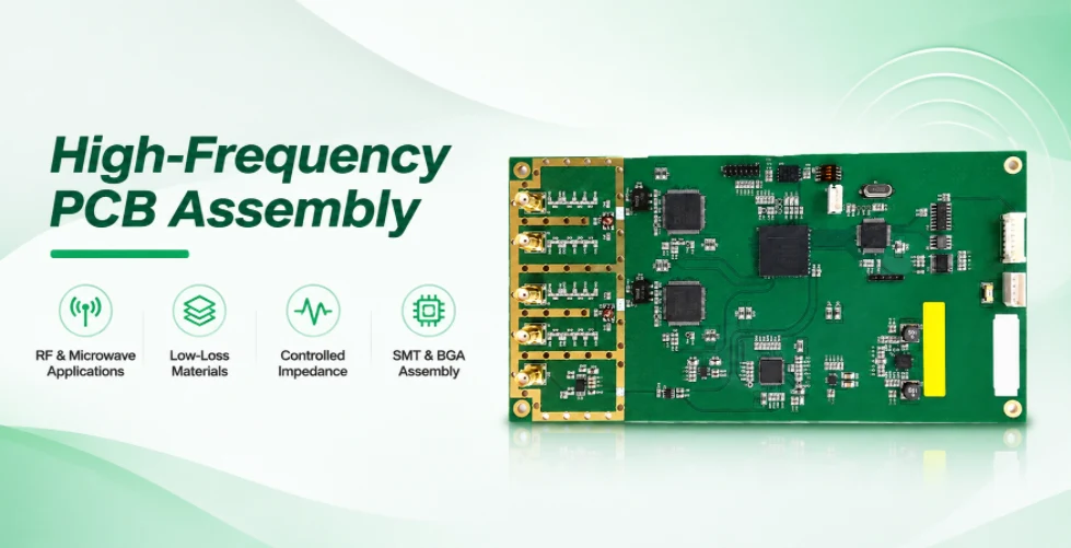
Highleap Electronics provides high frequency PCB assembly for RF, microwave and wireless electronic products, combining custom RF PCB fabrication, component sourcing, SMT population, RF connector installation and project-defined inspection and testing. Our build-to-print manufacturing scope covers RF front-end PCBAs, 5G wireless modules, microwave sensor boards, satellite communication electronics and mixed RF/digital assemblies. The approved laminate, layer structure, component list and acceptance specification determine how each board is made.
We coordinate bare PCB fabrication and assembly as one manufacturing project. This is particularly important for radio modules using Rogers or hybrid stack-ups, fine-pitch RF components, shield cans and coaxial interfaces, where PCB construction and assembly details must be aligned before production. Highleap can quote engineering samples, pilot lots and repeat orders, with optional material traceability and RF verification agreed for each project.
RF and Microwave PCB Assembly Services
Highleap supports custom RF and microwave PCBA manufacturing for OEM designs that require controlled PCB construction and repeatable assembly. The service can include radio-frequency and microwave PCB fabrication, approved electronic parts, SMT/THT assembly, shields, mechanical RF interfaces, inspection and specified functional checks.
A bare-board material certificate or successful power-on does not establish complete RF module performance; those criteria are determined by the equipment designer.
For combined analog and digital radio assemblies, one order may cover a low-loss antenna/RF section and a multilayer processor or control section. Highleap reviews the supplied PCB stack-up, RF interfaces, BOM, assembly drawing and test requirements together. Components and dielectric materials are not substituted merely because their headline specifications appear similar.
Manufacturing scope: Highleap manufactures to customer-approved files and can raise buildability questions during review. Antenna optimization, RF tuning, radio regulatory testing and specialized measurement fixtures should be included in the RFQ if required; they are not implied by the term PCB assembly.
5G RF PCB Assembly for Wireless Communication Equipment
For wireless infrastructure and connected products, Highleap can evaluate 5G RF PCB assembly and wireless communication PCBA using the approved RF design and component configuration. Relevant assemblies include sub-6 GHz 5G radio front-end boards, small-cell transceiver PCBAs, antenna-control modules, baseband/RF interface boards, Wi-Fi 6/6E and Wi-Fi 7 modules, GNSS receiver boards and industrial wireless gateways.
Wireless Communication PCBA Applications
RF switches, duplexers, filters, LNAs, amplifiers, matching passives and power-management circuitry.
RF ports, radio transceivers, control circuits and multilayer board integration.
Wireless interfaces, RF receiving circuits and antenna-related components.
Cellular modems, high-density processors, memory and Ethernet interfaces.
Such products can use different transmission-line constructions and shielding arrangements even when their manufacturing purchase order is consolidated.
High-Frequency Materials and Assembly Requirements
For wireless products with stringent insertion-loss or impedance requirements, our low-loss laminate and dielectric options can be reviewed against specified board materials, dielectric thicknesses and final copper geometry. Rogers, Taconic, Isola and other material families are candidates only when compatible with the released engineering design. Available stock and exact grades should be confirmed for each order.
| Assembly requirement | Manufacturing consideration |
|---|---|
| Fine-pitch components | Dedicated stencil apertures and controlled reflow |
| QFN packages | X-ray inspection of hidden solder joints where required |
| RF shielding | Shield placement and solder-joint requirements |
| Firmware and communication | Programming, board identification and link-level checks when specified |
These acceptance requirements for an assembled wireless module should be distinguished from bare-PCB electrical testing.
Microwave PCB Assembly for Radar and Satellite Electronics
Highleap can review microwave PCB assembly projects for radar, satellite communications and measurement hardware with operating-band-specific board and assembly requirements. Typical RFQs cover 24 GHz industrial radar modules, 60 GHz sensing electronics, 77–81 GHz automotive radar subassemblies, Ku/Ka-band satellite communication front ends, RF mixer/converter boards, phased-array support electronics and microwave test fixtures.
Microwave PCBA Manufacturing Requirements
| RF PCBA product | Fabrication and assembly priorities | Possible customer acceptance tests |
|---|---|---|
| 5G front-end / small-cell module | Low-loss multilayer PCB, shields, filters, antenna ports and programmed control | Power rails, RF path checks and approved radio-function test |
| Radar and microwave sensor | Launch, antenna geometry, dimensional registration and housing fit | Band-specific S-parameters or module checks |
| Satellite RF converter | Microwave laminates, connector repeatability and thermal dissipation | Gain, insertion/return loss and specified frequency sweep |
| RF measurement fixture | Defined reference planes, removable RF connectors and fixture geometry | VNA measurement with an approved calibration setup |
The board layout and customer qualification requirements govern which products can be manufactured and how they are accepted. For example, a 77 GHz radar board may require attention to antenna and launch geometry, solder-mask treatment, interconnect transitions and housing integration. A Ku/Ka-band front end may require controlled coaxial launch geometry and a specified insertion-loss or return-loss measurement range. These conditions cannot be confirmed by visual solder inspection alone.
Hybrid PCB Construction and RF Mechanical Interfaces
When microwave paths share a board with lower-frequency digital control, hybrid RF and FR-4 multilayer construction may offer a practical manufacturing approach if the customer approves the bonding materials and stack-up. The specified dielectric construction and copper profile must be maintained through fabrication, with routing, plating, solder-mask and connector features communicated to assembly before stencils and fixtures are finalized.
Radar or satellite assemblies may include edge-launch SMA/SMP connectors, press-fit interfaces, screws, metallic shields or thermal interface parts. The OEM should provide any required connector torque, mechanical alignment, calibration plane and RF port drawing. For regulated automotive, aerospace or satellite systems, PCB and PCBA workmanship records are only one part of the finished product’s qualification program.
Rogers PCB Assembly and High-Frequency PCB Materials
Rogers PCB assembly starts with the exact laminate and circuit construction, not just a generic request for a “Rogers board.” Highleap can evaluate Rogers RO4003C, RO4350B and other specified RF materials, including Rogers/FR-4 mixed constructions where approved, for RF front ends and high-frequency multilayer PCBAs. The confirmed material grade, core/prepreg combination, finished dielectric thickness and copper type belong in the fabrication drawing.
Material and Stack-Up Considerations
Different material systems do not share identical dielectric behavior, moisture response or processing recommendations. Material manufacturer data should inform the selected fabrication and soldering route.
A microstrip or grounded coplanar waveguide with a 50-ohm target depends on conductor width, dielectric thickness, copper finish and adjacent metal geometry. A nominal Dk from a datasheet does not replace approval of the production stack-up.
Controlled Impedance and Material Change Control
For controlled-impedance RF PCB manufacturing, specify target impedance, tolerance, relevant layers and coupon structures.
| Control item | Manufacturing requirement |
|---|---|
| Impedance target | Defined nominal value and tolerance |
| Signal layers | Specified impedance-controlled layers |
| Test coupons | Appropriate coupon structures for TDR verification |
| Material changes | Design-owner approval before production substitution |
TDR measurements help validate characteristic impedance on appropriate coupons or interconnects. They do not alone measure insertion loss, antenna gain or receiver noise figure. If the RF design has a specific return-loss or insertion-loss budget, its test method and fixtures must be separately defined.
Laminate source, acceptable copper-foil profiles and permissible prepreg changes should be controlled between first article and repeat orders. For programs with an approved RF layout, any proposed change in dielectric, trace geometry or plated finish should be reviewed by the design owner before it becomes a production substitution.
High-Frequency SMT Assembly and RF Connector Installation
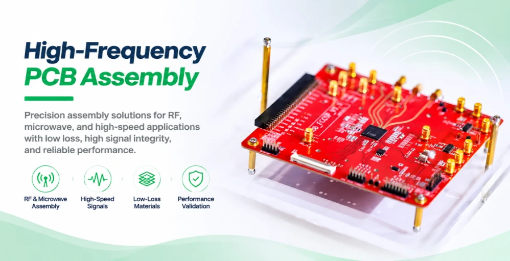
High-frequency SMT assembly requires precision placement and soldering, but also protects the electrical and mechanical details of the RF interface. Highleap provides SMT and mixed-technology board population for RF ICs, QFN devices, matching components, power amplifiers, filters, digital processors and through-hole RF or power connections. The route is selected from the package, board material and component geometry.
Small inductors and capacitors in a matching network may be sensitive to package parasitics and manufacturer tolerances. Highleap’s approved RF component sourcing should therefore follow exact manufacturer part numbers and the OEM’s substitution permissions. A value-equivalent passive is not necessarily equivalent in a tuned RF circuit. Moisture-sensitive packages, ESD-sensitive ICs and any restricted reflow exposure must be identified before assembly.
For processing or baseband areas, fine-pitch BGA and bottom-terminated IC assembly requires a suitable pad/via design, paste pattern and hidden-joint inspection plan. AOI helps inspect visible solder features; X-ray can support BGA/QFN inspection when agreed. Neither is a substitute for the customer-defined RF test.
RF connectors also deserve explicit instructions. SMA, SMP, MMCX and U.FL/I-PEX-type interfaces have different footprints, mating forces, soldering and retention conditions. Edge-launch pads and shield-ground joints must match the connector drawing. Where cable harnesses or shields are installed after SMT, establish the insertion sequence and any mechanical torque or alignment requirements.
RF PCB Testing and High-Frequency PCBA Quality Control
RF PCB testing is specified by the measurement: bare-board electrical test, TDR impedance verification, VNA S-parameters and active-module functional tests are different deliverables. Highleap’s RF testing and verification options can be reviewed for the released design, but measurement equipment, fixture availability, frequency range, sampling and report format must be confirmed for each project.
For passive lines, the OEM may specify S11 return loss or S21 insertion loss across a frequency sweep, with the calibration reference plane and connector configuration defined. A TDR result can reveal local impedance discontinuities, while VNA results characterize frequency-domain response under an appropriate setup. For active RF PCBAs, acceptable bias conditions, firmware state, gain, transmit power or receive sensitivity must be established by the owner of the RF specification.
Standard quality activities may include bare-board opens/shorts verification, fabrication inspection, first-article component checks, solder-paste/placement control, AOI and X-ray for hidden joints. These are useful manufacturing controls but they do not certify the completed radio for EMC, wireless regulations or a particular radar safety application. Highleap can integrate the requested evidence with PCB fabrication and turnkey assembly planning under one release package.
What should be recorded for repeat RF PCBA orders?
Useful production records may include approved PCB material and revision, BOM identity, critical RF connector part numbers, assembled serial or batch, functional test program and resulting measured limits. If the design has tuned component variants, distinguish each variant clearly in the BOM and test procedure. A pilot lot is valuable for establishing these controls before a production forecast is committed.
High-Frequency PCB Assembly Quote and Turnkey Manufacturing
Highleap can prepare a high-frequency PCB assembly quotation from a released RF PCB package, sourceable BOM and the required acceptance scope. The cost depends on laminate availability, multilayer construction, component packages, shields/connectors, special assembly fixtures, test coverage and the quantity and revision maturity. A Rogers or radar board that requires specialized RF measurement will not have the same cost structure as a standard FR-4 wireless controller.
For a meaningful RF PCBA RFQ, send:
- RF bare-board data: Gerber/ODB++, drill, stack-up, exact material grades, copper/finish, impedance and critical RF geometry drawings.
- Assembly data: BOM with MPNs and approved alternatives, CPL/centroid, assembly drawings, polarity, shields, coax connectors and hardware.
- Electrical requirements: operating bands, RF port definitions, important bias rails, controlled-impedance structures and test reference planes.
- Test and release: inspection criteria, test sweep/limits or functional procedure, measurement fixtures, firmware and any sampling or traceability requirements.
- Commercial scope: prototype or production quantities, delivery destination, consigned parts, target date and optional enclosure or cable integration.
Frequently asked RF manufacturing question — can Highleap deliver populated Rogers boards as well as bare RF PCBs? Yes, Highleap offers high-frequency PCB fabrication and PCBA services as a coordinated project. The exact material, connector, assembly and test requirements are evaluated against the released files.
Can a microwave board be quoted with only Gerber files? A preliminary fabrication review may be possible, but a complete populated RF assembly quotation needs the BOM, placements, mechanical interfaces and the intended quality/test scope.
Highleap Electronics — High-Frequency PCB & RF PCBA Manufacturing
Send your RF PCB stack-up, Gerber files, BOM, assembly drawings and RF test requirements. Highleap can review the fabrication, component sourcing, assembly and project-specific verification scope for an OEM quotation.

Recommended Posts

Power Electronics PCB Assembly for High-Current and Power Conversion Systems
Highleap Electronics provides Power Electronics PCB...

Automotive Electronics PCB Assembly: Traceability and Process Control
Highleap Electronics manufactures PCBs and provides...

Solar Inverter PCB Assembly for Power and Control Boards
If you are sourcing Solar Inverter PCB Assembly, Highleap...

PLC PCB Assembly for CPU, I/O and Communication Modules
Highleap Electronics provides PCB fabrication and PCB...
How to get a quote for PCBs
Let‘s run DFM/DFA analysis for you and get back to you with a report. You can upload your files securely through our website. We require the following information in order to give you a quote:
-
- Gerber, ODB++, or .pcb, spec.
- BOM list if you require assembly
- Quantity
- Turn time
In addition to PCB manufacturing, we offer a comprehensive range of electronic services, including PCB design, PCBA, and turnkey solutions. Whether you need help with prototyping, design verification, component sourcing, or mass production, we provide end-to-end support to ensure your project’s success.
For PCBA services, please provide your BOM (Bill of Materials) and any specific assembly instructions. We also offer DFM/DFA analysis to optimize your designs for manufacturability and assembly, ensuring a smooth production process.