
RF PCB Testing Techniques and Measurement Methods

RF PCB testing represents a critical phase in validating high-frequency circuit performance and ensuring manufacturing quality. As wireless communication systems operate at increasingly higher frequencies, the precision requirements for RF PCB testing become more stringent. Parameters such as insertion loss, return loss, and impedance matching must be measured with extreme accuracy to guarantee signal integrity across the entire frequency spectrum.
Unlike conventional PCB testing, RF measurements demand specialized equipment, controlled environments, and sophisticated calibration procedures to capture the subtle electrical characteristics that determine circuit functionality. This article explores the essential measurement parameters, testing instruments, and practical techniques that enable reliable RF PCB testing from prototype verification through volume production.
Importance of RF PCB Testing
RF PCB testing serves three fundamental purposes: design validation, manufacturing defect detection, and production consistency verification. The testing process differs significantly from standard PCB testing due to the critical nature of high-frequency signal propagation, where even minor impedance variations or dimensional tolerances can severely degrade performance.
While conventional PCB testing focuses primarily on DC continuity and basic functionality, RF PCB testing must evaluate complex electrical behaviors including signal reflection, transmission efficiency, and electromagnetic coupling effects. Applications such as antenna matching networks, RF filter assemblies, and power amplifier modules require rigorous testing protocols to ensure optimal performance at operating frequencies.
Common RF PCB Measurement Parameters
Insertion Loss and Return Loss
Insertion loss quantifies the signal power reduction as it passes through an RF circuit, directly indicating transmission efficiency. Return loss measures the reflected signal power resulting from impedance mismatches, with higher values indicating better matching and less energy waste. Both parameters are typically measured using a Vector Network Analyzer following comprehensive calibration procedures that eliminate systematic errors.
For most RF PCB testing applications, acceptable performance requires:
- Insertion loss – Minimized across the operational bandwidth, typically under 1-3 dB depending on circuit complexity and frequency range.
- Return loss – Should exceed 10 dB for basic applications, with more demanding systems requiring 15 dB or better to ensure proper impedance matching.
- Frequency consistency – Both parameters must remain stable across the entire specified bandwidth to prevent signal degradation.
Impedance and Phase Measurement
Characteristic impedance and phase response represent critical transmission line parameters that determine signal integrity in RF PCB testing applications. Impedance measurements verify that transmission lines maintain their designed values, typically 50 ohms or 75 ohms, within acceptable tolerances of ±5% or tighter for demanding applications.
Time Domain Reflectometry offers unique advantages for impedance profiling by identifying discrete discontinuities along signal paths. TDR measurements provide spatial resolution that frequency-domain techniques cannot achieve, making them invaluable for failure analysis and process optimization during RF PCB testing workflows.
S-Parameters (S11, S21, etc.)
S-parameters constitute the foundation of modern RF PCB testing, providing comprehensive characterization of multi-port network behavior. S11 describes input reflection while S21 represents forward transmission gain or loss, with S12 capturing reverse isolation and S22 indicating output match quality.
These measurements directly correlate with critical system performance metrics including amplifier gain, filter passband characteristics, and impedance matching effectiveness. Accurate S-parameter measurement during RF PCB testing requires proper port termination, verified calibration standards, and awareness of dynamic range limitations inherent to the test equipment configuration.

PCB Testing
Key Testing Instruments and Setups
Vector Network Analyzer (VNA)
The Vector Network Analyzer serves as the primary instrument for RF PCB testing, measuring both magnitude and phase relationships across specified frequency ranges. Modern VNAs employ sophisticated error correction algorithms to compensate for systematic measurement errors introduced by cables, connectors, and test fixtures.
Proper calibration using Short-Open-Load-Thru (SOLT) or Thru-Reflect-Line (TRL) standards remains essential for achieving accurate results. Port mismatch, cable stability, and connector repeatability represent common error sources that must be carefully managed throughout the RF PCB testing process to maintain measurement uncertainty below acceptable thresholds.
Time Domain Reflectometer (TDR)
Time Domain Reflectometry excels at detecting impedance discontinuities by transmitting fast-rising pulses and analyzing reflected waveforms. The technique proves particularly valuable during production testing and failure analysis when identifying specific physical locations of manufacturing defects such as via problems, trace width variations, or dielectric inconsistencies.
TDR measurements complement frequency-domain VNA data by providing intuitive spatial representation of impedance variations along transmission line structures. This capability enables rapid troubleshooting during RF PCB testing and qualification activities, reducing debug time compared to frequency-domain methods alone.
Spectrum Analyzer and Power Meter
Spectrum analyzers measure frequency content and spurious emissions critical for evaluating transmitter performance and regulatory compliance during RF PCB testing. These instruments capture nonlinear effects, harmonic distortion, and intermodulation products that S-parameter measurements alone cannot fully characterize in active circuit applications.
Power meters provide absolute power level measurements with calibrated accuracy, serving as reference standards for verifying amplifier output and system gain. Combined with VNA measurements, these instruments enable comprehensive RF PCB testing that validates both linear and nonlinear circuit characteristics.
Practical Techniques for Accurate Measurement
Test Fixture Design
Test fixture design profoundly influences RF PCB testing accuracy by introducing parasitic capacitance, inductance, and resistive losses between measurement ports and device connections. Minimizing fixture influence requires careful impedance matching, short electrical lengths, and robust mechanical stability to ensure repeatable contact resistance.
High-quality fixtures for RF PCB testing incorporate:
- Controlled impedance paths – Maintains 50-ohm environment from instrument ports to device-under-test connection points.
- Minimal transition discontinuities – Smooth transitions between connectors, fixtures, and PCB launch points reduce measurement artifacts.
- Mechanical repeatability – Consistent contact pressure and alignment ensure measurement stability across multiple insertions.
Calibration and De-Embedding
Calibration and de-embedding techniques mathematically remove fixture contributions from raw measurements, isolating true device performance from test system artifacts. Modern RF PCB testing employs multiple calibration approaches depending on fixture complexity and required accuracy levels.
Short-Open-Load-Thru calibration remains the most common method for coaxial systems, while Thru-Reflect-Line techniques better suit planar transmission line structures. De-embedding removes residual fixture effects that calibration cannot fully address, particularly important for millimeter-wave RF PCB testing where fixture electrical length becomes significant.
Environmental Control
Environmental control becomes increasingly critical as operating frequencies rise, with temperature variations affecting dielectric constant, conductor dimensions, and substrate properties. RF PCB testing laboratories typically maintain temperature stability within ±2°C and relative humidity between 40-60% to ensure consistent measurement results.
Cable management and connector care cannot be overstated during RF PCB testing operations. Damaged connectors or stressed cables introduce measurement uncertainty that can exceed device specification limits, requiring regular inspection protocols and careful handling procedures to maintain long-term measurement reliability.

Challenges in RF PCB Testing
Measurement Precision Requirements
High-frequency measurement demands extraordinary precision in instrumentation, connection hardware, and probe design to achieve meaningful results during RF PCB testing. Geometrical variations measuring only micrometers can produce significant impedance shifts at millimeter-wave frequencies, challenging both manufacturing tolerances and measurement resolution capabilities.
Test repeatability suffers when environmental conditions fluctuate or when connector wear degrades electrical performance over time. Establishing robust RF PCB testing procedures requires understanding these sensitivities and implementing appropriate control measures to maintain data integrity across production runs.
Cost and Efficiency Balance
The tension between engineering validation requirements and production testing economics creates ongoing challenges for RF PCB testing programs. Engineering teams require comprehensive characterization across temperature, frequency, and power conditions, while production environments demand rapid, cost-effective testing with minimal instrumentation investment.
Balancing these competing demands requires careful test plan development that identifies critical parameters warranting detailed measurement versus secondary characteristics acceptable for statistical process control monitoring. Effective RF PCB testing strategies optimize coverage while maintaining throughput requirements for manufacturing operations.
Best Practices for RF PCB Testing
Standardized Test Structures
Incorporating standardized test coupons alongside functional circuits enables statistical process monitoring without consuming production panels. These calibration structures provide consistent reference data for tracking manufacturing variations in impedance, loss tangent, and dielectric thickness across production lots during RF PCB testing campaigns.
Coupon designs should replicate critical transmission line geometries, via structures, and material stackups used in functional circuits. This approach ensures that RF PCB testing data accurately reflects the manufacturing quality of actual product features rather than simplified test patterns.
Simulation-Driven Optimization
Pre-production simulation and layout optimization reduce the likelihood of design-related failures during RF PCB testing, allowing measurement activities to focus on manufacturing quality rather than design debugging. Electromagnetic simulation tools predict circuit performance and identify potential issues before fabrication, minimizing costly iteration cycles.
Comprehensive data logging establishes the historical foundation for continuous process improvement and tolerance optimization in RF PCB testing operations. Recording measurement results with associated process parameters enables correlation analysis that identifies root causes of performance variations and supports data-driven manufacturing decisions.
Process Documentation
Establishing standardized measurement procedures and calibration schedules across all test stations ensures data consistency during RF PCB testing operations. Documented protocols should specify:
- Calibration frequency – Daily verification for production testing, with full calibration performed weekly or after equipment disturbance.
- Measurement sequence – Standardized test order prevents thermal drift effects and ensures comparable data across operators.
- Acceptance criteria – Clear pass-fail thresholds linked to electrical requirements rather than arbitrary measurement limits.
- Data retention – Long-term storage enables trend analysis and supports continuous improvement initiatives in RF PCB testing programs.
Conclusion
RF PCB testing represents the essential bridge connecting theoretical design performance with manufactured reality. Success requires deep understanding of measurement principles, proper instrumentation usage, and rigorous environmental control throughout the validation process. As wireless systems continue advancing toward higher frequencies and tighter specifications, disciplined RF PCB testing methodologies become increasingly critical for ensuring product reliability and performance.
Highleap Electronics provides advanced RF PCB fabrication and in-house testing capability, ensuring reliable high-frequency performance through precise impedance control and VNA-based validation. Our comprehensive testing protocols support both prototype development and volume production requirements.
Whether you’re optimizing signal integrity for RF modules or developing next-generation microwave systems, our engineering team can assist with material selection, controlled impedance design, and precision testing solutions. Contact Highleap Electronics to discuss your RF PCB testing or manufacturing needs today.

Recommended Posts
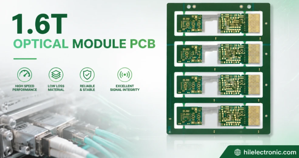
1.6T Optical Module PCB Manufacturing and Assembly Service
Table of contents1.6T Module Architectures and PCB...
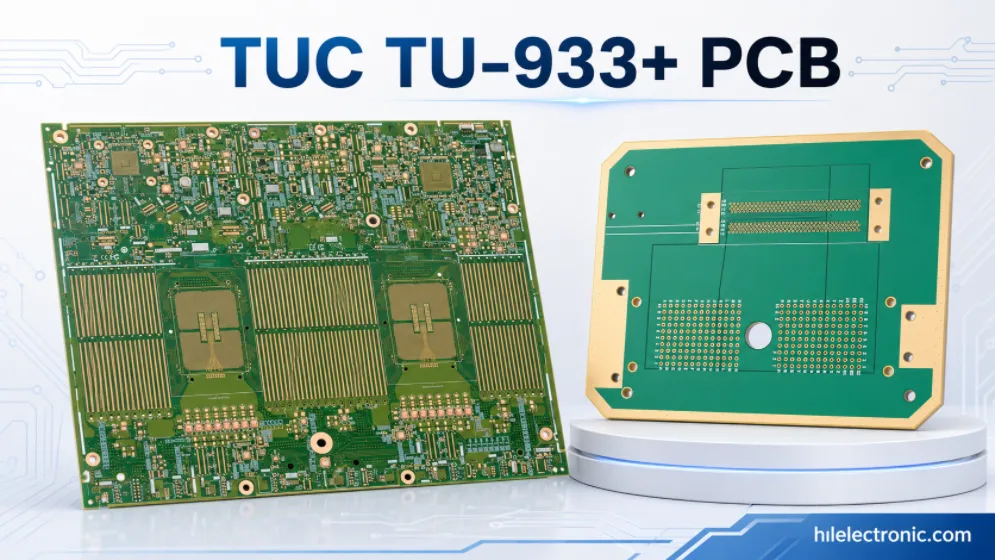
TUC TU-933+ PCB Manufacturing for Super-Low-Loss High-Speed Systems
Table of contentsWhat Is TU-933+ PCB Material?Why TU-933+...
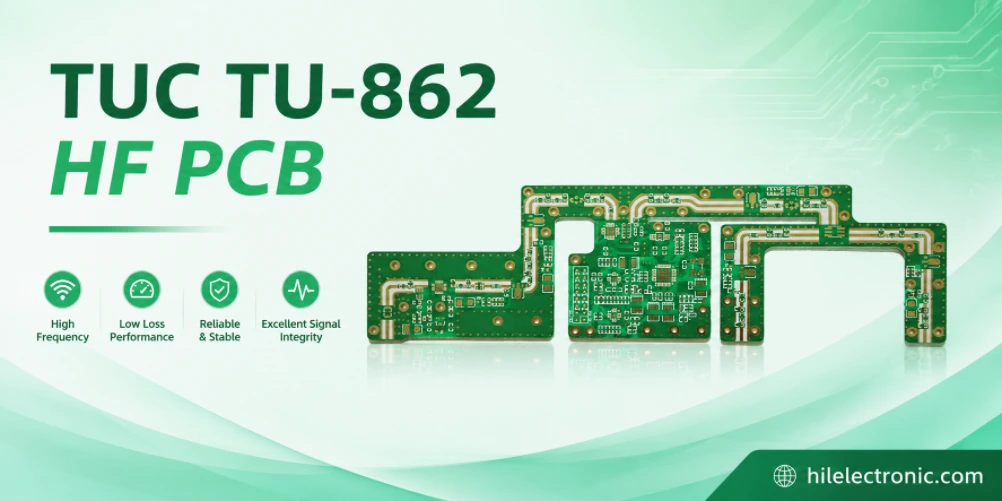
TUC TU-862 HF PCB Manufacturing and Assembly Service
Table of contentsWhat Is TU-862 HF?Why Choose TU-862 HF...
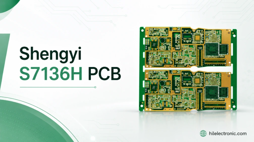
Shengyi S7136H PCB Manufacturing and Assembly Service
Table of contentsWhat Is a Shengyi S7136H PCB?Why...
How to get a quote for PCBs
Let‘s run DFM/DFA analysis for you and get back to you with a report. You can upload your files securely through our website. We require the following information in order to give you a quote:
-
- Gerber, ODB++, or .pcb, spec.
- BOM list if you require assembly
- Quantity
- Turn time
In addition to PCB manufacturing, we offer a comprehensive range of electronic services, including PCB design, PCBA, and turnkey solutions. Whether you need help with prototyping, design verification, component sourcing, or mass production, we provide end-to-end support to ensure your project’s success.
For PCBA services, please provide your BOM (Bill of Materials) and any specific assembly instructions. We also offer DFM/DFA analysis to optimize your designs for manufacturability and assembly, ensuring a smooth production process.