
EV Charger PCB Assembly Services
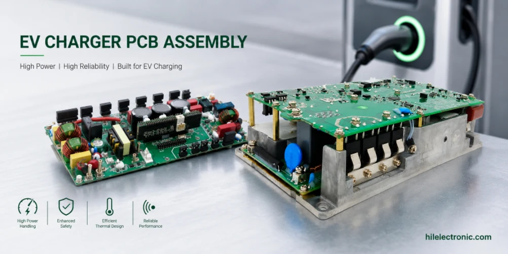
Table of Contents
Highleap Electronics provides EV charger PCB assembly services for charging control boards, power control boards, communication boards, display or interface boards and related electronic subassemblies. We manufacture PCBs and assemble PCBAs according to customer design files, BOMs, drawings and test requirements. We do not certify the complete EV charger, charging station, cable set or installation. Product compliance, system safety and final certification remain the responsibility of the charger manufacturer or product owner.
EV charger electronics can include high-voltage interfaces, control circuits, metering, communication modules, relays, contactors, current sensing, thermal monitoring, protection circuits and connector interfaces. A reliable assembly program needs accurate BOM control, PCB fabrication quality, soldering control, connector handling, spacing protection, inspection and customer-defined test procedures.
For related projects, see BMS PCB assembly, power electronics PCB assembly and heavy copper PCB assembly.
EV Charger PCB Assembly Service Scope
Supported charger board types
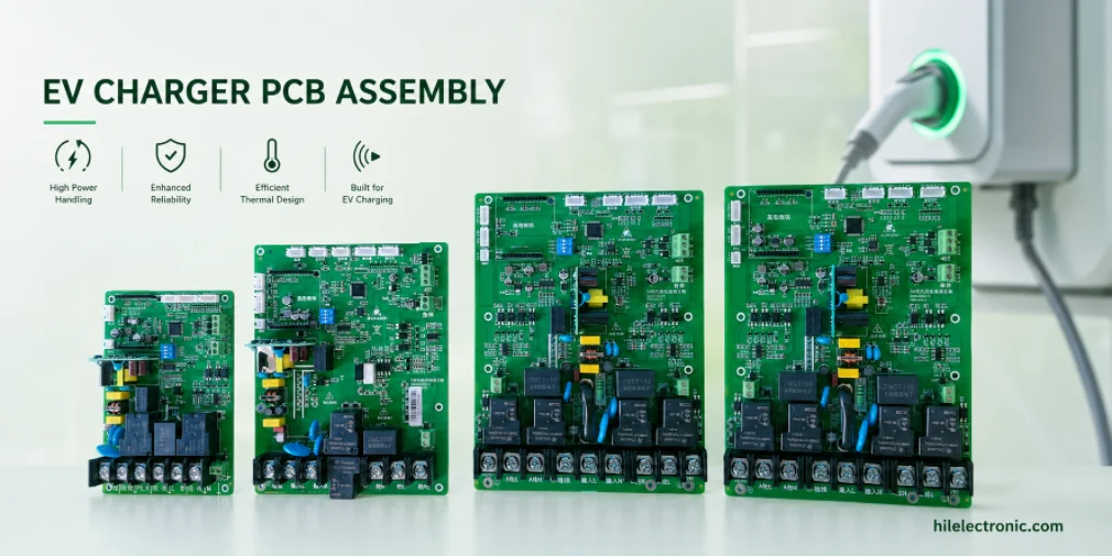
Highleap can support EV charger PCBA builds when the manufacturing files are complete and the assembly requirements are within agreed capability. Charger systems may include AC input boards, control logic boards, communication boards, display boards, relay control boards, metering boards, pilot signal boards and auxiliary power boards. DC charger power modules and high-power assemblies may require additional process review due to heat, current and insulation requirements.
MCU, communication, sensing, relay drive and safety monitoring circuits.
High-current connectors, relays, contactors, terminals and sensing paths.
CAN, RS-485, Ethernet, cellular, Wi-Fi or customer-specified interfaces.
LED indicators, displays, buttons, touch modules or interface connectors.
PCB fabrication and assembly integration
EV charger electronics often combine PCB fabrication requirements with assembly requirements. The PCB may need controlled copper thickness, creepage slots, high-voltage spacing, plated holes, solder mask openings and mechanical mounting features. The assembly may need connectors, relays, sensors, transformers, heat-generating components and selective inspection. Coordinating fabrication and assembly helps avoid conflicts between board design, component fit and final assembly.
Standards and compliance boundary
EV supply equipment may be designed around market-specific standards such as IEC 61851 for conductive charging systems, UL requirements, regional grid rules and customer safety requirements. Highleap does not certify the complete charger. We can manufacture and assemble the PCBA to the approved files and support customer-specified inspection or test steps when the procedures and acceptance criteria are provided before production.
Power Stage and Control Board Assembly
Relay, contactor and terminal assembly
Power interface boards may include relays, contactors, terminal blocks, current sensors, fuses, shunts, transformers or large connectors. These parts need correct footprint, soldering method, mechanical support and inspection criteria. Heavy components should not rely only on solder joints when mechanical stress is expected; mounting hardware or design support should be defined by the customer when needed.
Control electronics and low-voltage circuitry
Control boards often include microcontrollers, isolated power supplies, communication transceivers, memory, indicators, watchdog circuits and input/output protection. SMT assembly should protect component orientation, package matching, solder joint quality and ESD-sensitive handling. If programming is required, the customer should supply firmware, programming interface details and version verification method.
Mixed assembly planning
- PCB review: confirm stackup, copper, spacing, slots and finish.
- BOM review: confirm power parts, connectors, package types and alternates.
- SMT build: assemble small components and inspect critical polarity.
- Through-hole process: assemble terminals, relays, transformers and connectors.
- Final inspection: check solder joints, mechanical seating, labels and customer-defined tests.
High-Voltage Spacing and Creepage Considerations
Customer-defined spacing requirements
High-voltage spacing is a design responsibility that must be translated into manufacturable PCB features. The customer should define creepage, clearance, slots, coating, copper pullback and isolation boundaries based on the applicable product standard, operating voltage, pollution degree, material group and product environment. Highleap can manufacture the specified features but should not be expected to infer safety spacing from a generic note.
Slots, cutouts and coating boundaries
Slots and cutouts can increase creepage distance or separate high-voltage regions when defined by the design. Their width, length, tolerance, plating status and edge quality should be included in the fabrication drawing. If conformal coating is used, coating keepout areas around connectors, test pads, switches and mating surfaces should be defined. Coating cannot be treated as a late manufacturing addition when it affects inspection, rework and safety spacing.
Isolation component assembly
Optocouplers, digital isolators, isolation transformers and isolated power modules may have specific package spacing and orientation requirements. The assembly drawing should show correct placement and polarity. If a component has multiple pin-compatible alternatives with different insulation ratings or package dimensions, approved alternates should be controlled in the BOM.
Thermal Management and Heavy Copper Requirements
Heat-generating components
EV charger boards may include MOSFETs, diodes, relays, current sensors, resistors, transformers, regulators and connectors that generate heat. Thermal performance depends on the product design, copper area, PCB material, airflow, enclosure, heat sink and load profile. During assembly, pad design, solder paste, component seating and inspection help protect the intended thermal path.
Heavy copper and current paths
Some EV charger boards require heavy copper or wide copper areas for current carrying and heat spreading. Current capacity is not determined by copper weight alone; it also depends on trace width, temperature rise, airflow, layer position, board thickness, copper planes and environment. If heavy copper is required, the stackup should identify copper thickness by layer and the drawing should define any special plating, finished thickness or tolerance requirements.
| Thermal item | Design data needed | Manufacturing impact |
|---|---|---|
| Heavy copper | Copper weight by layer, current path and temperature rise target. | Etching, soldering thermal balance and board thickness control. |
| Thermal vias | Via size, pitch, fill/cap requirement and thermal pad strategy. | Plating, solder wicking and inspection planning. |
| Heat sink interface | Mounting holes, keepouts, flatness and interface material. | Mechanical fit and final assembly control. |
Link to high-current manufacturing support
For boards where copper thickness, current paths or thermal vias dominate the manufacturing plan, see heavy copper PCB assembly for high-current electronics.
Connector, Relay and Power Component Assembly
Connector fit and mechanical stability
EV charger PCBAs often use large connectors, terminal blocks, board-to-wire connectors, board-to-board connectors and harness interfaces. The assembly drawing should define orientation, mating direction, pin 1, latch direction and height restrictions. Large connectors should be reviewed for solder joint stress and mechanical support. If connector torque, retention or mating force matters, acceptance criteria should be supplied by the product owner.
Relay and contactor control areas
Relays and contactors can require large pads, strong solder joints and spacing from heat-sensitive components. Drive circuits and sense circuits should be assembled with correct values and polarity. If a relay part has multiple coil voltage options or package variants, the BOM should define the exact MPN and approved alternates. Wrong variants can pass basic footprint review but fail electrical function.
Power component inspection
Inspection should focus on solder fill, alignment, pin seating, heat damage, flux residue, mechanical clearance and labeling. X-ray may be useful for selected hidden solder joints or thermal pads when required by the customer. Functional testing should be based on customer-provided procedure because EV charger system behavior depends on firmware, interlocks, sensors and full product architecture.
Functional Testing and Safety-Related Checks
PCBA-level inspection
PCBA-level inspection can include incoming material review, solder paste inspection, AOI, X-ray for selected components, visual inspection, polarity check, continuity check and first article approval. These checks confirm assembly quality, but they do not replace charger certification or system validation. If the customer needs hipot, insulation resistance, firmware programming or communication checks at PCBA level, procedures and acceptance limits should be defined before quotation.
Programming and communication verification
EV charger boards may need firmware loading, calibration files, communication checks or serial number programming. The customer should provide programming tools, files, access method and pass/fail criteria. If the board communicates with other modules, standalone PCBA testing may be limited unless the customer provides a fixture or system simulator.
Documentation for regulated products
Chargers sold into regulated markets may require product-level documentation, component approval, safety testing and certification. Highleap can provide agreed manufacturing records such as inspection reports, test logs, material or assembly records and certificate of conformance when included in the order scope. Certification reports for the complete charger must be handled by the product owner or certified test body.

Recommended Posts

TMM4 Filter PCB Manufacturing
TMM4 filter PCB manufacturing is controlled by the...

TMM3 PCB Manufacturing for RF Modules
TMM3 PCB manufacturing is most useful where the RF module...

TMM6 PCB Fabrication
TMM6 fabrication is the process-control page for a mid-Dk...

TMM10 PCB Manufacturing for Compact RF Designs
Table of contentsHow TMM10 Shrinks RF StructuresTMM10 vs...
How to get a quote for PCBs
Let’s run DFM/DFA analysis for you and get back to you with a report. You can upload your files securely through our website. We require the following information in order to give you a quote:
-
- Gerber, ODB++, or .pcb, spec.
- BOM list if you require assembly
- Quantity
- Turn time
For PCBA services, please provide your BOM (Bill of Materials) and any specific assembly instructions. We also offer DFM/DFA analysis to optimize your designs for manufacturability and assembly, ensuring a smooth production process.