
Smart Bracelet PCB Manufacturing and Assembly
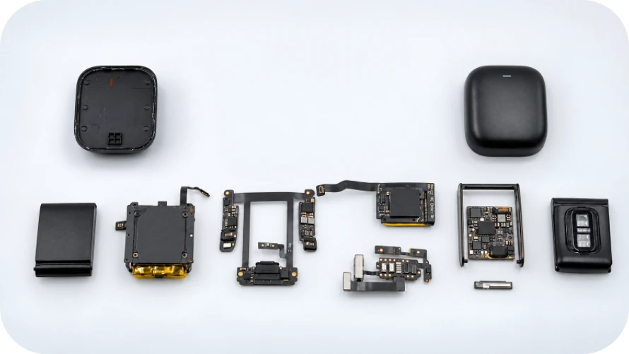
Highleap Electronics supports customer-designed smart bracelet electronics through electronic manufacturing services that can include PCB fabrication, flex or rigid-flex manufacturing, component sourcing, SMT/THT assembly, programming, inspection and customer-defined functional testing. Application security, payment or credential certification, antenna tuning, algorithms and finished-product regulatory validation remain project-specific OEM responsibilities unless separately defined.
Smart Bracelet PCB Requirements and Application Architecture
The first manufacturing decision is to identify what the bracelet actually does. A display-free NFC access band may prioritize coil geometry, secure components and low standby current. A BLE notification bracelet may focus on antenna clearance, haptic drive and battery life. A sensor-heavy wearable adds IMU, optical sensing, temperature measurement, display or other functions that increase placement and test complexity.
| Bracelet type | Design priority | Manufacturing focus |
|---|---|---|
| NFC access / ID bracelet | NFC antenna, secure IC, low standby power | Coil geometry, tuning BOM, credential/test boundary |
| BLE-connected bracelet | Phone connectivity, battery life, haptics | RF keep-out, matching parts, current and functional test |
| Sensor wearable | IMU, optical sensors, display or multi-sensor integration | Placement, cleanliness, power rails and test coverage |
| Enterprise / mixed-function bracelet | NFC, BLE, sensors and application-specific I/O | Variant control, firmware mapping and repeatable production test |
This architecture decision also controls cost. A simple rigid PCB can be appropriate when all electronics fit in one protected module. Flex, rigid-flex or HDI should be added only when the enclosure, package density or distributed functions justify them. For buyers, that means the most useful quotation is based on the actual board construction and feature set rather than a generic wearable price.
Smart Bracelet Flex, Rigid-Flex and Mechanical Integration
Bracelet geometry often determines whether the electronics can stay on one rigid board or must be distributed along the band. A central rigid PCB is usually the simplest option. A flex PCB manufacturing approach becomes useful when sensors, antennas, buttons or charging contacts must sit away from the main module. Rigid-flex PCB manufacturing can reduce connector count and assembly height when rigid component zones and flexible interconnect must be integrated into one structure.
Separate static and dynamic bend zones
A flex section formed once during enclosure assembly has different reliability requirements from a section that moves every time the bracelet is worn. Dynamic regions need controlled bend radius, trace direction and strain relief. Components, vias and rigid-flex transitions should stay out of high-strain zones unless the construction is specifically designed for that motion.
Control battery and charging interconnects
Battery tabs, welded joints, board connectors and flex conductors must carry both average and peak current without transferring mechanical load into fragile pads. If the battery supplier changes, tab geometry, pouch construction and conductive materials should be reviewed because they can affect fit, assembly sequence and nearby RF performance.
Treat the antenna region as mechanically controlled
A bracelet may use a chip antenna, a PCB antenna or an antenna section integrated into the flex. NFC may also use a band-integrated loop. Antenna keep-outs, stiffeners, metal hardware and enclosure geometry should be frozen together so DFM changes do not unintentionally move copper or mechanical materials into an RF-controlled area.
NFC, BLE, Sensors and Power on a Smart Bracelet PCB
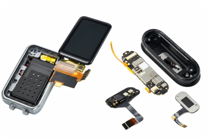
NFC, BLE, sensors and power management should be reviewed as one product system because they share board area, battery capacity and mechanical space. The PCB factory can preserve the released layout and test each defined function, but final antenna tuning, application security and algorithm validation remain product-level engineering responsibilities.
BLE and NFC require different antenna controls
A Bluetooth PCB design typically relies on a 2.4 GHz antenna, feed and matching network with a defined ground reference and keep-out. NFC uses an inductive loop whose dimensions, turns, tuning capacitance and nearby metal strongly affect coupling. For bracelet products using NFC, the NFC antenna PCB geometry, ferrite or shielding materials and tuning components should be treated as controlled parts of the assembly.
Same-value RF passives should not be substituted automatically. Parasitics, tolerance and Q can change the tuned response. Production BOM rules should identify approved alternates, and BLE/NFC functions should be verified separately because a successful BLE connection does not prove NFC performance.
Sensors, display and haptics add placement and current constraints
IMUs should be mounted in a mechanically representative location. Optical sensors need accurate placement, clean apertures and enclosure alignment. Displays and vibration motors create current transients that should not disturb sensitive sensor references or RF areas. The assembly drawing should show sensor windows, connector insertion direction and any coating or adhesive keep-outs.
Design production checks around real power states
Standby current may dominate an access-control bracelet, while BLE bursts, optical LEDs, displays or haptics can dominate active current in a feature-rich product. A battery management PCB or charging circuit should therefore be reviewed with both sleep and peak-current conditions in mind. Production fixtures can screen customer-defined current limits, charging behavior and obvious leakage, while total runtime still depends on firmware and battery capacity.
Smart Bracelet PCB Fabrication and PCBA Manufacturing
Once the electrical and mechanical architecture is stable, the manufacturing question becomes whether the released design can be fabricated, assembled, inspected and repeated at the required yield. Highleap Electronics provides PCB assembly services for customer-designed products, including sourcing, SMT/THT assembly, inspection, programming and customer-defined functional tests.
Match PCB technology to package density
A simple bracelet may use a conventional two- or four-layer rigid PCB. Denser BLE, secure or display designs may need additional layers or HDI. QFN, BGA, LGA and other bottom-terminated packages require controlled stencil printing, reflow and inspection. X-ray is useful when hidden joints create a real manufacturing risk, but it should be selected because the package needs it rather than as a generic quality claim.
Control RF, NFC and security-sensitive BOM items
RF matching components, ferrite parts, secure ICs and application-specific devices need explicit alternate rules. A structured component sourcing process should preserve do-not-substitute items and keep the approved BOM tied to the PCB, firmware and test revision.
Use fixtures where thin flex cannot support itself
Thin flex can move during printing, placement, reflow and test. Carrier panels or reusable fixtures can stabilize the assembly and protect antenna, sensor and exposed-contact areas. The same fixture strategy should consider depanelization and handling so the flex is not creased after a good soldering process.
Define charging contacts as product interfaces
Pogo-pin pads or exposed charging contacts may have specific finish, outline and wear requirements. They should be identified in fabrication and assembly drawings rather than treated as ordinary test pads. Cleaning, coating and handling instructions must keep these surfaces free of residue.
Useful files for a manufacturing review
- Gerber or ODB++ and released board outline data.
- BOM with manufacturer part numbers and approved alternates.
- Pick-and-place and assembly drawings.
- Flex/rigid-flex stack-up, bend zones and stiffener information when applicable.
- BLE/NFC antenna keep-outs and mechanically controlled areas.
- Programming package and customer-defined functional-test requirements.
- Target prototype, pilot or production quantities.
These files do not all need to be complete before the first conversation. The purpose of an early manufacturing review is to identify what is missing before tooling, sourcing or production commitments make changes expensive.
Smart Bracelet Reliability and Production Quality Control
A smart bracelet is repeatedly worn, removed, charged and exposed to skin moisture. Reliability therefore depends on the PCB construction, assembly process and enclosure working together. A generic “wearable grade” label is less useful than defining the actual stresses the product must survive.
| Stress | Typical risk | Production control |
|---|---|---|
| Sweat / humidity | Corrosion, leakage, contaminated contacts | Cleaning, sealing interface and coating/masking where specified |
| Repeated bending | Copper fatigue, pad or transition cracking | Defined bend zones, strain relief and handling limits |
| Shock / drop | Battery, connector or heavy-component damage | Mechanical support and controlled component placement |
| Charging cycles | Contact wear, joint stress, local heating | Contact inspection, mechanical support and thermal validation |
Conformal coating helps, but does not make the bracelet waterproof
A conformal-coating manufacturing process can protect selected circuitry from humidity and contamination, but the product still depends on enclosure seals, band interfaces, sensor windows and charging contacts. Coating drawings should define masking around antennas, NFC loops, optical sensors, connectors and exposed contact surfaces.
Production test should screen repeatable failures
The exact test depends on the bracelet. Useful checks can include programming, sleep and active current, BLE communication, NFC response, sensors, display/haptic operation and charging. Secure credential provisioning should be treated as a separate controlled scope when required. The goal is not to reproduce full product qualification on every PCBA, but to catch manufacturing defects with repeatable acceptance criteria.
From Prototype to Volume Production: Choosing a Smart Bracelet PCB Assembly Partner
A production-ready smart bracelet is not created by scaling the prototype quantity alone. The prototype should confirm the mechanical stack, antenna environment, flex forming, charging interface and test access. Pilot builds should then use production-intent materials, components, fixtures and firmware so yield and cycle-time data are meaningful.
Use prototype and pilot builds to remove production uncertainty
- Form the flex in the real bracelet and check for pad or transition stress.
- Verify BLE and NFC in the final enclosure with the intended battery and nearby metal.
- Confirm programming and functional-test access after the assembly is formed.
- Replace temporary debug connectors or pads with a production test strategy.
- Freeze the BOM, firmware mapping and variant matrix before repeat orders.
Track yield by process stage
Bare-board electrical test, SMT, flex forming, connector or battery operations, BLE/NFC checks and final function should be tracked separately. If one bend, package or contact dominates failure, stage-level yield data makes the root cause visible. A single final-test number does not show where cost and rework are being created.
Choose a supplier that can preserve the released baseline
The manufacturing partner should be able to manage rigid, flex or rigid-flex fabrication, fine-pitch assembly, controlled sourcing, programming, fixtures and production testing while keeping BOM, firmware and hardware revisions aligned. Highleap Electronics can support the transition into high-volume PCB assembly after the production baseline is approved.
Common buyer questions
Does every smart bracelet need flex or rigid-flex PCB?
Can BLE and NFC be used on the same bracelet PCB?
What is needed to start a smart bracelet PCBA quote?
Can conformal coating make a smart bracelet waterproof?
Highleap Electronics supports customer-designed smart bracelet PCB and PCBA builds with PCB fabrication, flex or rigid-flex manufacturing, component sourcing, SMT/THT assembly, programming, inspection and customer-defined functional test. Start with the project data you already have and refine the production package during review.

Recommended Posts

TMM4 Filter PCB Manufacturing
TMM4 filter PCB manufacturing is controlled by the...

TMM3 PCB Manufacturing for RF Modules
TMM3 PCB manufacturing is most useful where the RF module...

TMM6 PCB Fabrication
TMM6 fabrication is the process-control page for a mid-Dk...

TMM10 PCB Manufacturing for Compact RF Designs
Table of contentsHow TMM10 Shrinks RF StructuresTMM10 vs...
How to get a quote for PCBs
Let’s run DFM/DFA analysis for you and get back to you with a report. You can upload your files securely through our website. We require the following information in order to give you a quote:
-
- Gerber, ODB++, or .pcb, spec.
- BOM list if you require assembly
- Quantity
- Turn time
For PCBA services, please provide your BOM (Bill of Materials) and any specific assembly instructions. We also offer DFM/DFA analysis to optimize your designs for manufacturability and assembly, ensuring a smooth production process.