
Taconic RF-35 PCB 价格及制造报价
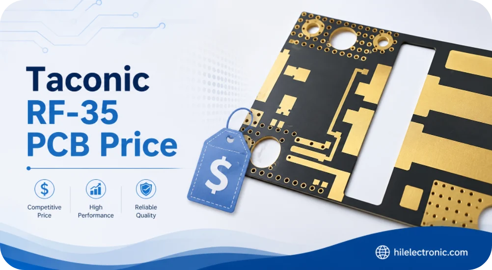
Highleap Electronics provides itemised Taconic RF-35 PCB price quotations for bare boards and complete RF assemblies. Quotes cover prototype, NPI, low-volume and repeat production, with separate visibility for material procurement, RF fabrication, quality documentation, component sourcing, assembly, testing, packaging and international delivery.
RF-35 pricing cannot be reduced to a board-area formula because the material is a legacy designation and the process depends on thickness, copper, RF tolerances, PTH requirements and available stock. Highleap verifies the released construction first, then provides a firm commercial route rather than a low headline price followed by material or expedite surcharges.
RF-35 Material and Supply Factors Behind the Price
The largest RF-35 cost uncertainty is often the material route rather than the etched circuit area. A quotation must distinguish verified legacy stock, customer-supplied laminate and a customer-approved alternative. Each route has a different purchase quantity, documentation burden, yield risk and delivery schedule.
| 价格驱动因素 | 商业效果 | How Highleap controls it |
|---|---|---|
| Exact laminate and thickness | Nonstandard or legacy constructions may require special procurement or minimum purchase quantities. | Confirm the controlled grade, thickness, copper and certificate before issuing a firm quote. |
| RF geometry and tolerances | Tighter line, gap, registration and finished-thickness controls increase engineering and inspection effort. | Quote against the critical-dimension table and actual acceptance limits. |
| PTH and mechanical complexity | Dense via fences, connector holes, cavities and tight routing tolerances add drilling, plating and dimensional control. | Separate standard fabrication from special process steps. |
| Assembly and test scope | RF connectors, shields, controlled cleaning, fixtures and RF verification can exceed bare-board cost. | Itemise PCBA, NRE, test preparation and recurring test charges. |
For cross-material budgeting, Highleap can also compare 罗杰斯PCB制造 and RF-35 routes, but the comparison is returned with separate qualification assumptions rather than as an automatic substitution.
Taconic RF-35 PCB Price: What the Highleap Quote Includes
RF-35 is a legacy Taconic designation within the material business now operated by AGC Multi Material. Highleap checks the AGC/Taconic business history and the current AGC RF laminate portfolio when confirming whether the requested construction is current stock, legacy stock, customer-supplied material or subject to an approved transition.
Commercial Scope Available in One Quote
| 项目区 | Highleap项目支持 |
|---|---|
| 材料 | Verified laminate route, thickness, copper, certificate and procurement allowance |
| 裸PCB | CAM, tooling, fabrication, electrical test, agreed RF/impedance evidence and final inspection |
| 组装 | Component sourcing, stencil/NRE, SMT/THT, RF connectors, shielding and workmanship inspection |
| 测试与验证 | Programming, fixtures, functional test and customer-defined RF measurements when specified |
| Delivery | Packing, split shipment options, freight assumptions and destination requirements |
| 售后服务 | Lot traceability, nonconformance response, record review and controlled repeat-order support |
Highleap刚性射频PCB制造能力
The published factory limits below define Highleap’s rigid-PCB process envelope for quotation. They are not automatic promises that every extreme can be combined in one RF-35 build; material availability, copper, panel utilisation, RF tolerances and assembly scope are reviewed together before price and delivery are confirmed. See the complete Highleap刚性PCB能力表 按照已公布的工厂规格执行。
| 制造品 | 已发布的Highlap能力 | RF/PTFE项目条件 |
|---|---|---|
| 最大层数 | 最多 60 层 | 特定 RF/PTFE 或混合堆叠的层数在层压、对位、过孔和材料审查后得到确认。 |
| 最小内层走线/空间 | 2/2 密耳(0.05/0.05 毫米) | 释放的射频几何形状还取决于铜厚度、箔类型、蚀刻补偿和关键尺寸公差。 |
| 最小外层痕迹/空间 | 2/2 密耳(0.05/0.05 毫米) | 精细的射频间隙和耦合结构需要针对具体项目制定可行性和检验标准。 |
| 板材厚度范围 | 0.2–8.0毫米 | 指定 Taconic/AGC 结构的可用厚度取决于层压板厚度、粘合方法和经批准的叠层结构。 |
| 板材厚度公差 | 低于 1.0 毫米时为 ±0.1 毫米;高于 10 毫米时为 ±1.0%。 | 射频连接器发布和外壳接口应明确说明任何更严格的产品级要求。 |
| 最小成品板材尺寸 | 10×10毫米 | 小型电路可能需要以制造面板或阵列的形式交付,以便进行制造和组装。 |
| 最大成品板材尺寸 | 22.5 × 47.5 英寸(571.5 × 1206.5 毫米) | 大尺寸 PTFE 板材需要单独审核材料板材尺寸、套准、平整度、布线和运输。 |
| 最小机械钻孔/环形环 | 0.15 mm / 0.127 mm | 最终过孔设计取决于电路板厚度、长宽比、电镀要求和材料特定的钻孔工艺。 |
| 最小激光钻孔/环形环 | 0.075 mm / 0.075 mm | 激光微孔的设计需经过介质厚度、捕获焊盘设计、铜层构建和顺序层压等审核。 |
| 机械钻头纵横比 | 最多20:1 | RF/PTFE 结构可实现的比例必须通过最终的孔径、板厚和电镀要求来确认。 |
| 激光钻孔纵横比 | 1:1 | 微孔几何形状只有在堆叠结构和可靠性审查之后才会公布。 |
| 最大内/外铜 | 最多 10 盎司 | 最大铜含量不能自动与最精细的线条/空间或所有 PTFE 结构相结合。 |
| PTH/NPTH耐受性 | PTH ±0.075 mm;NPTH ±0.05 mm | 连接器和射频接地孔应标明成品直径以及任何更紧密配合的要求。 |
| 轮廓容差 | ±0.1毫米 | 边缘开口、腔体、插槽和连接器位置可能需要专门的尺寸控制方案。 |
| 受控阻抗容差 | 单端和差分:≤50 Ω 时误差为 ±5 Ω;高于 50 Ω 时误差为 ±7% | 所列公差适用于已批准的堆叠方式、优惠券策略和测量方法。 |
| 可选表面处理 | ENIG、ENEPIG、OSP、HASL、浸银、浸锡、闪金、硬金和金手指 | 表面处理的选择需考虑射频损耗、焊接、导线键合、连接器接触和环境要求。 |
功能组合通知: 表格中的数值为各工厂的产能极限。层数、2/2 mil 厚度、10 oz 铜、最大面板尺寸、20:1 长宽比以及最薄的电路板结构并非假定能够同时实现。Highleap 会在审核具体的材料、叠层结构、铜层厚度、钻孔、射频容差、表面光洁度和组装方案后,确认可用的组合。
An RF-35 PCB price from Highleap covers the complete released manufacturing route, not only a square-area laminate calculation. The quotation can include material procurement, CAM, test coupons, tooling, imaging, etching, drilling, PTFE hole preparation, plating, solder mask, surface finish, routing, electrical test, inspection, reports, assembly, testing, packing and international freight assumptions.
| Quotation block | Included cost drivers | What the buyer receives |
|---|---|---|
| 材料 | Approved grade, thickness, copper, minimum buy, freight, certificates and usable panel area | A stated material route and any legacy-stock or alternative-approval condition. |
| 加工制作 | Layer count, image count, etch tolerance, drilling, plating, hybrid pressing and mechanical features | A price tied to the actual Gerber, drawing and quality plan. |
| 品质 | Electrical test, impedance coupons, microsections, dimensional reports, first article and traceability | Defined evidence instead of an undefined “high quality” statement. |
| 组装 | BOM value, sourcing, stencil, setup, placement, soldering, inspection, programming and test | Bare-board and PCBA pricing from one controlled dataset. |
| Delivery | Expedite level, split shipment, packaging, Incoterms and destination | A committed schedule and commercial delivery basis. |
For general cost principles, Highleap’s high-frequency PCB cost guide explains why RF material, copper profile, tolerance, panel utilisation and inspection can dominate the final unit price. The RF-35 quotation applies those factors to the actual project rather than publishing a misleading fixed online price.
The Eight Inputs That Change RF-35 Cost Most
- Material status: legacy stock, customer-supplied material, special purchase or approved alternative have different commercial risks.
- Dielectric thickness and tolerance: nonstandard cores can create minimum purchase quantities and longer material lead time.
- 铜箔: weight, ED/RA type and surface profile affect material price, conductor loss and etch behaviour.
- Board area and panel utilisation: irregular outlines, RF launches and coupon requirements may reduce pieces per panel.
- RF geometry tolerance: narrow lines, tight gaps, coupled structures and phase-matched networks require tighter process control.
- Hole and via structure: dense ground vias, small finished holes, blind/buried structures and filled vias add operations and inspection.
- Finish and final treatment: ENIG, immersion silver, tin, OSP, selective finishes, edge plating and connector preparation differ in cost.
- Evidence and test: impedance, microsection, PIM, insertion loss, dimensional Cpk or custom RF test must be defined and priced.
Highleap returns clear assumptions through the same commercial discipline described in accurate PCB budgetary quotations. A budgetary figure can be prepared from dimensions, layer count, thickness, copper, quantity and key processes, but a firm price requires fabrication data and a released material route.
Avoiding False Economy in an RF-35 Quote
A lower quote is not commercially equivalent when it omits legacy-material procurement, impedance evidence, RF connector assembly, test fixtures or shipment documentation. Highleap aligns quotations to the same scope and can explain the trade-off between material utilisation, panel quantity, inspection level and delivery risk. See the high-frequency PCB cost guide for the broader cost model.
For assembled products, the BOM may exceed the bare-board cost. Long-lead RF semiconductors, connectors, filters, shields and precision passives should be reviewed separately from laminate pricing. Highleap can provide customer-supplied, consigned or turnkey component models according to the procurement strategy.
How Highleap Reduces Cost Without Weakening the RF Design
Cost-down work begins with panel and process efficiency, not an uncontrolled material downgrade. Highleap reviews the design with the customer and identifies changes that preserve the approved electrical model.
| Cost-down option | 潜在益处 | Approval condition |
|---|---|---|
| Improve panelisation | More finished boards per production panel and lower material waste | Outline, tooling rails and assembly panel requirements must remain acceptable. |
| Use a standard available thickness | Lower MOQ and shorter material procurement | RF geometry must be recalculated and design owner must approve. |
| Relax nonfunctional tolerances | Reduce process controls and yield loss | Only dimensions without electrical, assembly or interface impact. |
| Consolidate drill sizes | Reduce drill changes and tooling complexity | Annular ring, current, grounding and connector requirements remain satisfied. |
| Optimise coupon and report scope | Avoid duplicate evidence | Customer quality and contractual requirements remain fully covered. |
| Combine PCB and PCBA sourcing | Reduce logistics, duplicate inspection and supplier coordination | One frozen dataset controls fabrication and assembly. |
| Forecast repeat demand | Reserve material and improve purchase economics | Revision control and consumption forecast are stable. |
Highleap will also quote an approved comparison route when requested. The RF-35 versus RO4350B comparison explains why nominally similar Dk does not make two laminates interchangeable. Electrical modelling, PTH processing, flame rating, thickness options and qualification status must all be considered.
Prototype, NPI, and Volume Price Structures
RF-35 prototype price includes a larger share of one-time engineering, material purchase and setup because those costs are spread across few boards. NPI pricing adds first-article control, assembly learning, inspection review and potential fixture development. Volume pricing can improve through panel optimisation, reserved material, repeat tooling, stable BOM sourcing and scheduled releases.
| Order stage | 商业目标 | Recommended quote format |
|---|---|---|
| 原型 | Obtain functional boards quickly with sufficient evidence | One or two quantities, expedited option, material status and minimum test package. |
| NPI / engineering validation | Prove repeatability and assembly process | Separate bare board, first assembly, fixture/NRE and remaining build. |
| 试生产 | Validate yield, test and logistics | Quantity breaks plus first-article and process-capability requirements. |
| 量产 | Control landed cost and continuity | Forecast pricing, scheduled releases, material reservation and change control. |
| Aftermarket / legacy support | Maintain an older design with limited demand | Material availability plan, small-batch setup and last-time-buy discussion. |
Assembly is quoted with a separate cost breakdown when useful. Buyers can compare setup, placement, soldering, inspection and test using Highleap’s PCB assembly cost factors and request the exact PCBA package through the PCB assembly quotation service.
RF-35 Lead Time and Expedite Charges
Expedite charges are only meaningful after the critical path is known. For RF-35, material availability may be more important than fabrication capacity. Highleap first confirms stock or an approved procurement route, then assigns fabrication, assembly and test milestones.
A quotation timeline starts after complete files are received. Highleap first closes material and engineering questions, then confirms fabrication, assembly and test capacity. Expedited cost is quoted only for the steps that actually require priority scheduling; unavailable material cannot be solved by charging an artificial rush fee.
- Standard schedule: planned engineering, material procurement and production using the normal factory route.
- Expedited fabrication: priority CAM and production scheduling where material and process capability are ready; see 快速PCB服务.
- 分批发货: bare boards or first assembled articles ship before the balance when the project benefits from early validation.
- Customer-supplied material: can shorten procurement only after incoming identity, dimensions, quantity and condition are accepted.
- Alternative material route: may shorten delivery but requires written design-owner approval and any necessary requalification.
The quotation states the committed shipment date, assumptions and items that can move the date. Highleap does not use “fastest lead time” as a blanket claim for every RF-35 construction.
Send the Files Required for a Firm RF-35 Price
For a firm quotation, send Gerber/ODB++, fabrication drawing, stackup, material TDS or controlled callout, copper, drill/route data, impedance or RF geometry, finish, panel requirements, quantity breaks, delivery location and quality reports. Add BOM, centroid, assembly drawings, firmware and test specification for PCBA. Submit through Highleap 快速报价 or contact Highleap engineering.
相关的 RF-35 PCB manufacturing page describes fabrication, material control, assembly and after-sales support. For projects where RF loss and geometry are the primary concerns, review RF-35 high-frequency PCB production.
Can Highleap quote RF-35 PCB price from a drawing only?
A budgetary price may be possible, but a firm quote requires the fabrication data, approved material route, copper, finish, quantity and quality requirements.
Does a larger quantity always reduce unit price?
Usually setup and material utilisation improve, but special material MOQ, yield, inspection, assembly test time and forecast stability also affect the result.
Can Highleap quote both RF-35 and RO4350B?
Yes when alternatives are permitted. Each route will identify material, process, delivery, price and qualification assumptions separately.
Is after-sales support included?
Highleap supports revision and lot traceability, manufacturing-record review, containment, failure-analysis coordination and corrective-action response for delivered orders.
What files produce the most accurate RF-35 PCB price?
Gerber or ODB++, fabrication drawing, stackup, drill and route data, material and copper specification, critical RF dimensions, quantity, target delivery, BOM, centroid, assembly drawings and test requirements.
Can Highleap provide a cost-reduction proposal?
Yes. Highleap can review panel utilisation, standard material thickness, copper, tolerances, inspection scope, split delivery and assembly packaging. Any electrical or material change is returned for customer approval before it is included in the quote.

推荐文章

Taconic RF-35 PCB制造服务——从原型到批量生产
图 1. Taconic RF-35 PCBTaconic RF-35 是主力机型……

Isola Astra MT77 PCB制造
图 1. Isola Astra MT77 PCB 制造 Isola Astra...

定制 Rogers RO4835 PCB 制造和组装服务
图 1. Rogers RO4835 PCB Rogers RO4835 PCB 是一款……

Nelco N4000-13 PCB材料和制造指南 | Highleap Electronics
图 1. Nelco N4000-13 PCB Nelco N4000-13 PCB 是一款……
如何获取 PCB 报价
我们将为您进行DFM/DFA分析,并尽快向您提供报告。您可以通过我们的网站安全上传文件。为了给您报价,我们需要以下信息:
-
- Gerber、ODB++ 或 .pcb,规格。
- 如果需要组装,请提供 BOM 清单
- 数量
- 转弯时间
如需 PCBA 服务,请提供您的 BOM(物料清单)和任何具体的装配说明。我们还提供 DFM/DFA 分析,以优化您的设计,提高可制造性和装配性,确保生产流程顺畅。