
8-layer PCB Standard Stacking Technology and Design Challenges
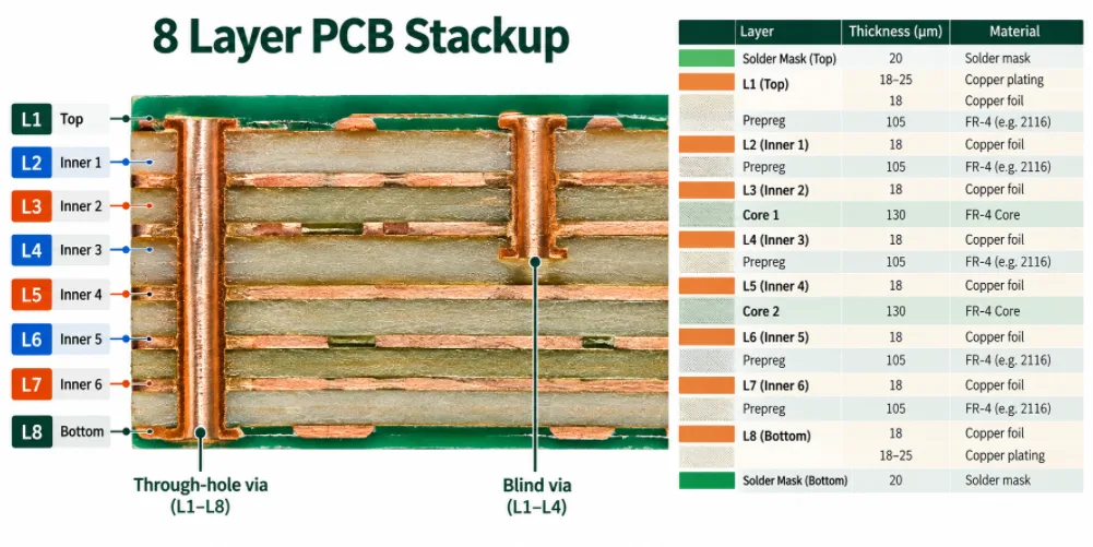
An 8-layer PCB provides additional routing capacity for high-speed digital systems, industrial controls, networking equipment and complex electronic products. However, adding copper layers alone does not guarantee better electrical performance or easier manufacturing. The result depends on layer assignment, dielectric construction, reference-plane continuity, via structures and manufacturing tolerances.
For hardware engineers and OEM purchasing teams, the objective is to develop an eight-layer construction that meets electrical requirements without introducing unnecessary manufacturing complexity. Highleap Electronics provides PCB fabrication and PCB assembly services, supporting projects from engineering review through production. This guide explains the stackup decisions, fabrication challenges and quotation requirements that matter before an 8-layer PCB enters production.
8 Layer PCB Stackup and Manufacturing Guide
1. 8 Layer PCB Stackup Design for Manufacturing
An 8-layer PCB stackup must do more than accommodate eight copper layers. It needs to provide suitable signal reference planes, sufficient routing space, practical power distribution and a balanced construction that can be manufactured within the required tolerances. For PCB buyers, the stackup should therefore be reviewed as both an electrical design and a manufacturing specification before the board enters production.
How to Arrange the Eight Copper Layers
A typical eight-layer board may use four signal layers and four ground or power-related layers, although the actual allocation depends on routing density, interface requirements and power-distribution needs. One possible starting configuration is:
| Layer | Example Assignment | Main Consideration |
|---|---|---|
| L1 | Top signal | Component connections and critical external routing |
| L2 | Ground plane | Reference path for L1 signals |
| L3 | Internal signal | Routing density and reference continuity |
| L4 | Power plane | Power distribution and clearance requirements |
| L5 | Ground plane | Reference continuity and plane allocation |
| L6 | Internal signal | Routing capacity and impedance requirements |
| L7 | Ground plane | Reference path for bottom-layer signals |
| L8 | Bottom signal | Component connections and external routing |
This is an illustrative layer assignment, not a universal eight-layer manufacturing standard. Some designs require a different allocation of signal, ground and power layers. The final arrangement should reflect the critical interfaces, power architecture, routing constraints and required electrical performance.
For high-speed designs, the relationship between adjacent signal and reference layers deserves particular attention. When a signal changes layers through a via, its return-current path must remain practical. A poorly planned transition can increase electromagnetic interference or degrade signal integrity, even when the trace geometry itself appears acceptable.
Dielectric Thickness and Controlled Impedance
Controlled impedance depends on trace width, copper thickness, dielectric properties and the distance between the signal conductor and its reference plane. Differential routing also requires consideration of pair spacing and the surrounding dielectric structure.
A trace routed over a nearby ground plane will generally require different geometry from one with a greater reference-plane separation. Consequently, a generic eight-layer construction should not automatically replace the stackup used during signal-integrity design.
Before fabrication, the engineer and manufacturer should confirm:
- Target single-ended and differential impedance values and tolerances.
- The reference layer associated with each critical signal layer.
- Required dielectric thicknesses and laminate properties.
- Finished copper thickness and trace geometry.
- Whether impedance coupons, testing and reports are required.
If the proposed material or dielectric construction differs from the original design, the resulting impedance should be reviewed before the change is approved. Any adjustments to trace geometry or stackup should be documented rather than made without customer authorization.
Core, Prepreg and Finished Board Thickness
An eight-layer PCB is typically constructed from copper-clad cores and prepreg bonding materials. Their combination affects finished thickness, dielectric spacing, lamination behavior and material availability.
A nominal finished thickness of 1.6 mm may suit some eight-layer designs, but it should not be assumed to be appropriate for every board. Connector engagement, enclosure dimensions, component placement and electrical requirements may impose different constraints.
The manufacturing review should confirm finished thickness and tolerance, copper weight for each layer, core and prepreg construction, and any application-specific thermal or electrical material requirements. These constraints must be satisfied together rather than optimizing one parameter in isolation.
What Highleap Reviews Before Fabrication
For a production-ready eight-layer PCB, the stackup review should connect the electrical design to the actual manufacturing requirements. This includes checking layer assignments, material specifications, dielectric spacing, drilling constraints, copper clearances and finished board thickness.
If the design includes dense BGA routing, blind or buried vias, backdrilling or other special processes, these features should be reviewed alongside the proposed layer construction. They may influence manufacturing sequence, process capability, lead time and cost.
Highleap Electronics can review the supplied fabrication files and stackup requirements as part of a project-specific manufacturing assessment. See our PCB layer stackup service and PCB material selection guide for related engineering information.
The objective is to identify potential conflicts before production tooling is released, so the quoted board construction reflects the intended electrical performance and manufacturing requirements.
2. Key Manufacturing Challenges in 8 Layer PCB Fabrication
Eight-layer PCB fabrication requires coordinated control of internal layer registration, lamination, drilling and finished board geometry. These factors become especially important when the design contains dense BGA escape routing, small capture pads, tight clearances or controlled-impedance signals.
Internal Layer Registration and Drilling
All copper layers must remain aligned within the specified manufacturing tolerances. Misregistration can reduce annular-ring margins, affect clearances and compromise via reliability. The risk increases when the design combines small pads, dense drilling patterns and limited copper spacing.
Before production, the manufacturer should review drill-to-copper clearances, annular-ring requirements and the registration margins required by the selected construction. Blind vias, buried vias and backdrilling should be specified clearly because they can introduce additional process requirements.
Lamination Quality and Board Flatness
Core and prepreg selection, resin flow, copper distribution and lamination control influence the quality of the finished multilayer construction. Inadequate process control can contribute to internal defects or dimensional instability.
Board bow and twist also deserve attention when the PCB must fit a mechanical enclosure or pass through SMT reflow. A symmetrical stackup is a useful starting point, but copper distribution, material properties, board geometry and thermal exposure also affect flatness.
Impedance and Production Consistency
The stackup used in the design must correspond to the construction used in manufacturing. Unreviewed changes to laminate, dielectric spacing or copper geometry can affect impedance and make the fabricated board inconsistent with the original electrical assumptions.
For controlled-impedance projects, agree on target values, tolerances, verification methods and reporting requirements before production. Where material substitutions or stackup adjustments are proposed, obtain engineering approval before implementation.
3. 8 Layer PCB Manufacturing Cost and DFM Review
The cost of an eight-layer PCB depends on more than its layer count. Board dimensions, laminate selection, copper thickness, drilling requirements, via structures, surface finish, tolerances, testing and order quantity all influence the final quotation.
Where Manufacturing Costs Can Be Reduced
- Review via complexity: Use conventional plated through-holes when the electrical and routing requirements permit them. Advanced via structures should solve a defined design problem.
- Confirm material requirements: Specify a particular laminate when its electrical, thermal or reliability properties are necessary. Qualify alternatives before accepting substitutions.
- Set practical tolerances: Apply tight dimensional, drilling and impedance requirements where the design needs them, rather than restricting every feature unnecessarily.
- Improve panel utilization: Review board dimensions, array configuration and order quantities while preserving assembly handling and testing requirements.
- Compare equivalent quotations: Confirm that every supplier is pricing the same stackup, copper weights, surface finish, testing scope and delivery terms.
Cost optimization should not come at the expense of signal integrity, reliability or the approved manufacturing specification. The most useful savings are those that remove unnecessary complexity while preserving the board’s functional requirements.
Information Needed for an Accurate Quote
To reduce quotation delays, prepare the Gerber or ODB++ files, NC drill data, stackup drawing, board dimensions, finished thickness, copper weights, laminate requirements, surface finish and order quantity. Include controlled-impedance specifications and special-process requirements where applicable.
Ask the manufacturer to identify any assumptions, exclusions or proposed alternatives in writing. For repeat production, also clarify price breaks, one-time engineering charges and the point at which the quoted lead time begins.
For additional budget planning, see our PCB fabrication cost guide. A complete specification makes it easier to compare suppliers on the same manufacturing basis.
4. 8 Layer PCB Fabrication and Assembly Services
For products requiring populated circuit boards, fabrication and assembly should be considered together. Component footprints, BGA placement, panelization, solder mask, surface finish and test access can affect assembly even when the bare PCB meets its specifications.
Highleap Electronics provides PCB manufacturing and PCB assembly services for multilayer electronic products. Depending on project requirements, the scope can include PCB fabrication, component sourcing, SMT and through-hole assembly, AOI, X-ray inspection and functional testing.
Before releasing a PCBA order, prepare the BOM, pick-and-place data, assembly drawings and applicable testing instructions. Confirm the board revision and component specifications so fabrication and assembly are based on the same approved design.
For integrated production support, explore our turnkey PCB assembly service and PCB assembly capabilities.
Request an 8 Layer PCB Quote
Send Highleap Electronics your PCB files, stackup requirements, order quantity and target delivery date. Our team can review your fabrication and assembly requirements for a project-specific quotation.

Recommended Posts

Racing Wheel Controller PCB Manufacturing & Assembly for Force-Feedback and Direct-Drive Gaming Systems
Highleap Electronics provides PCB fabrication and PCBA for...

FR4 Dielectric Constant Calculator and PCB Design Guide
How to get a quote for PCBs Let's run DFM/DFA analysis for...

GPS Sports Watch PCB Design: GNSS, RF, Sensors and PCBA Manufacturing
Turning a compact GPS sports watch controller from an...

Cellular Modem PCB: From Module Carriers to PCBA
Need a manufacturer for a cellular modem PCB or a fully...