
PCB Annular Rings: Design Guidelines

PCB annular rings are the copper areas that remain around drilled holes. They are essential for plated-through holes, vias, and component leads because they provide electrical connection area and tolerate normal manufacturing variation in drilling and registration.
Annular ring design should be based on the finished hole, pad geometry, layer registration, and the fabrication capability agreed for the job.
Table of contents
- What Is a PCB Annular Ring?
- How to Calculate Annular Ring
- Why Annular Rings Matter
- Common Annular Ring Issues
- IPC and Fabrication Tolerances
- Vias and Component Holes
- Teardrop Pads and Annular Rings
- DFM Checks for Annular Rings
- Inspection and Test
- Annular Ring Design Review With Highleap
What Is a PCB Annular Ring?
For a plated-through hole, the annular ring is the radial copper land surrounding the finished hole. It supports plating continuity and provides a solderable or connectable area. On inner layers, adequate capture is also needed to maintain a reliable barrel connection after drilling.
The required ring differs by board class, layer type, feature density, and whether the hole is a via, component lead, tooling feature, or specialized structure.
How to Calculate Annular Ring
A simple nominal calculation is annular ring = (pad diameter – finished hole diameter) / 2. The design value must also allow for drill wander, registration tolerance, plating, and any customer acceptance requirement.
Use the finished hole in the calculation when that is the controlled drawing value. Confirm whether the fabricator needs a larger drill size to achieve that finished result after plating.
Why Annular Rings Matter
An undersized ring increases the risk of breakout, reduced plating capture, weak solder joints, and yield loss. The impact can be greater on dense multilayer boards where inner-layer registration tolerance consumes a larger part of the available land.
Choosing a slightly larger pad where routing allows can improve fabrication margin and reduce unnecessary risk.
Common Annular Ring Issues
Typical problems include drill-to-pad misregistration, insufficient inner-layer capture, pads reduced by routing or thermal relief geometry, and land sizes copied from an incompatible design rule set. A nominally correct CAD rule can still be unsuitable for the actual stack-up and board class.
Review exception areas such as connectors, press-fit holes, heavy copper regions, and fine-pitch breakout zones separately.

IPC and Fabrication Tolerances
IPC documents and customer specifications define acceptance concepts, but the target class and contractual requirements must be established for each product. Fabrication capability, drill size, board thickness, layer count, and registration all influence the practical land requirement.
Use the manufacturer design rules for the intended process and treat them as part of the released fabrication package.
Vias and Component Holes
Vias may use smaller pads to preserve routing density, while component holes may require larger lands for soldering and mechanical strength. High-current or mechanically loaded connections need special consideration for pad size, hole size, plating, and strain relief.
Do not apply one annular-ring value blindly across every hole type.
Teardrop Pads and Annular Rings
Teardrops smoothly widen the connection between a trace and pad. They can improve copper retention near a drilled hole and add margin in selected areas, but they do not replace a properly sized annular ring or a suitable drill tolerance.
Use them where they fit the routing and manufacturing strategy, then verify that the resulting geometry is clean and does not create spacing violations.
DFM Checks for Annular Rings
A DFM review should examine finished-hole sizes, pad stacks, drill files, layer registration, annular-ring exceptions, and clearance around every hole type. The review is particularly valuable after a footprint library change, stack-up revision, or panelization update.
Correcting marginal pads before tooling avoids costly rework and can improve first-pass yield.

Inspection and Test
Fabrication inspection can include automated optical inspection, X-ray or microsection analysis where appropriate, and electrical testing for continuity and isolation. The method should be selected from the risk and acceptance criteria rather than used as a substitute for sound design rules.
Document any critical holes or coupons that require additional verification.
Annular Ring Design Review With Highleap
Highleap Electronics can review annular-ring rules, drill data, stack-up, and special-hole requirements before fabrication. Clear information about the product class and critical features helps focus the review on the real manufacturing risks.
For a manufacturability review, request a PCB quote with the Gerber files, drill files, drawings, and fabrication notes.
Get a Free PCB & PCBA Quote

Recommended Posts

PCB Current Calculator: Sizing Trace Width and Vias with the IPC-2221 Formula
Figure 1. Pcb Current Calculator reference image for PCB...

Microphone PCB Design: How the Board Itself Shapes Your Audio Quality
Figure 1. Microphone Pcb reference image for PCB...

Board-to-Board Connector: Types, Specifications, and How to Select One
Figure 1. Board To Board Connector reference image for PCB...
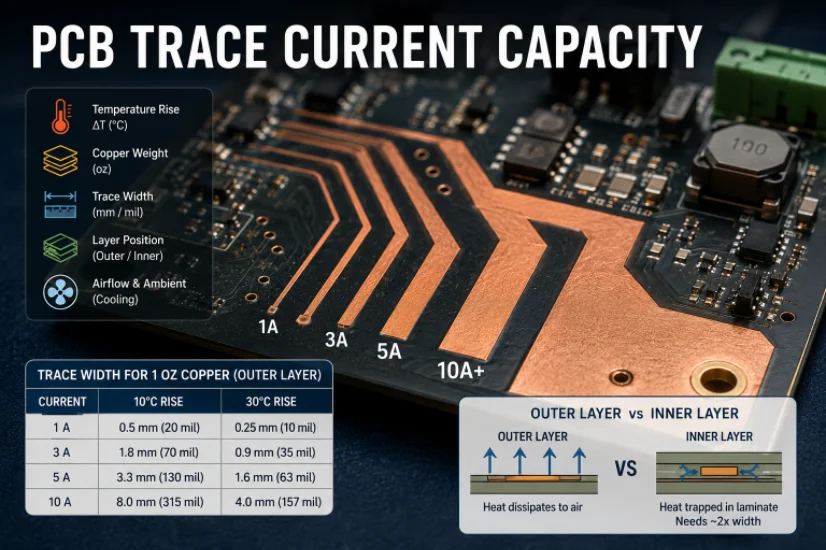
PCB Trace Width Calculator: How to Size Traces for Current, Voltage Drop, and Impedance
Figure 1. A PCB trace width calculator is a starting point...
How to get a quote for PCBs
Let us run DFM/DFA analysis for you and get back to you with a report.
You can upload your files securely through our website.
We require the following information in order to give you a quote:
-
- Gerber, ODB++, or .pcb, spec.
- BOM list if you require assembly
- Quantity
- Turn time
In addition to PCB manufacturing, we offer a comprehensive range of electronic services, including PCB design, PCBA (Printed Circuit Board Assembly), and turnkey solutions. Whether you need help with prototyping, design verification, component sourcing, or mass production, we provide end-to-end support to ensure your project’s success. For PCBA services, please provide your BOM (Bill of Materials) and any specific assembly instructions. We also offer DFM/DFA analysis to optimize your designs for manufacturability and assembly, ensuring a smooth production process.