
Chromebook PCB Manufacturing and Assembly for OEM Mainboards
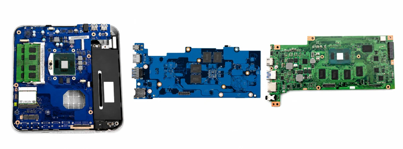
Table of contents
- From Chromebook PCB Architecture to a Controlled Manufacturing Package
- Chromebook PCB High-Speed Routing, Memory and Display Interfaces
- USB-C, Charging, Wireless and Peripheral Integration
- Power Distribution and Thermal Density on Compact Mainboards
- Multilayer Fabrication, HDI and Fine-Pitch Requirements Where Needed
- BGA/SMT Assembly and Inspection for Chromebook Mainboards
- Functional Test, NPI and Repeat-Production Control
- Selecting a Chromebook PCB Manufacturing and Assembly Partner
A Chromebook PCB is normally discussed as the main motherboard that carries the computing, memory, storage, power-management and core I/O functions of a ChromeOS device. ChromeOS hardware exists in different processor platforms and form factors, so a manufacturer should not assume one fixed board architecture, layer count or component set.
Highleap Electronics supports customer-designed boards from released fabrication data through PCB assembly, approved component sourcing and customer-defined testing. The manufacturing task is to preserve the customer’s electrical and mechanical intent while controlling dense packages, high-speed nets, power conversion and revision-sensitive options.
Additional interface boards, USB boards or flex interconnects may be present in some designs, but they are architecture choices rather than a defining feature of every Chromebook. This article therefore focuses on the mainboard and treats secondary assemblies only where the released product data requires them.
1. From Chromebook PCB Architecture to a Controlled Manufacturing Package
The mainboard typically concentrates the application processor or processor platform, memory, storage, wireless connectivity, display links, audio, camera interfaces, charging and system power. The exact partitioning varies by platform. A safe RFQ begins with one controlled release rather than a generic “Chromebook motherboard” description.
Architecture definition matters because the board shop and assembler only see part of the system context. Processor platform, memory technology, storage topology, embedded-controller responsibilities, port count and mechanical envelope can all change escape routing, power sequencing, connector placement and test access. The production package should therefore identify not only the PCB revision but also the BOM variant, fitted/DNI options, firmware image and any platform-specific assembly notes that are necessary to build that exact configuration.
Manufacturing package
| Customer input | Manufacturing use | Control point |
|---|---|---|
| Gerber/ODB++ and fabrication drawing | Defines layer data, drills, outline and stack-up notes | Do not infer impedance or via structure from the schematic alone. |
| BOM and approved alternates | Defines fitted components and variants | Keep processor-platform and power parts tied to the released revision. |
| Pick-and-place and assembly drawing | Controls orientation and fitted options | Resolve DNI and alternate-footprint conflicts before setup. |
| Mechanical data | Controls connector, heatsink and chassis relationships | Check board outline, mounting holes and component keep-outs. |
| Firmware/test instructions | Defines programming and acceptance checks | Separate visual inspection from functional verification. |
DFM boundary
A PCB DFM review can identify manufacturability questions, but it should not silently redesign processor routing, memory topology or power architecture. Those remain controlled by the customer’s released design.
For OEM programs, the practical conversion point is a manufacturable release package. Before material is committed, engineering and procurement should be able to answer four questions: which stack-up is released, which parts are truly approved, which mechanical dimensions are installation-critical, and which functions must be demonstrated before shipment. If those answers are still distributed across emails or prototype notes, consolidating them before NPI usually prevents more risk than adding inspection after the fact.
A manufacturing package for a Chromebook-class mainboard should describe more than the bare PCB. The BOM, placement data, fabrication drawing, assembly drawing, mechanical outline, firmware reference and test plan need to identify the same released hardware. Processor-platform options can change memory population, storage devices, wireless modules, connector sets or power circuitry while the board outline remains similar. Without explicit option control, purchasing and assembly can build a physically correct board with the wrong fitted configuration.
DFM review should therefore separate design intent from factory-controlled characteristics. The customer defines electrical architecture, stack-up targets, critical net classes, approved components and acceptance criteria. The manufacturer verifies whether drill structures, annular rings, solder-mask clearances, copper balance, panelization, component spacing and assembly access are producible. This boundary is important because a fabricator should not silently change a high-speed escape, power-via field or connector datum simply to make fabrication easier.
- Tie every SKU to one BOM/CPL/firmware/test revision rather than relying on purchase-order descriptions.
- Identify controlled-impedance nets and any coupon or reporting requirement in the fabrication package.
- Provide mechanical data for heat spreaders, shields, speakers, cameras and USB-C openings when these constrain assembly.
- Define customer-approved alternates before shortages occur; platform-sensitive ICs should not be substituted by value/package alone.
2. Chromebook PCB High-Speed Routing, Memory and Display Interfaces
Dense computing boards can contain DDR memory buses, high-speed storage links, USB, display interfaces and other timing-sensitive nets. Fabrication must preserve the released dielectric construction, reference-plane continuity, copper geometry and via implementation used by the layout team.
High-speed manufacturing control starts with preserving the assumptions used during layout. A memory bus may be sensitive to length matching, skew, reference-plane continuity and via count, while storage or display links may be limited by a different loss or impedance budget. These are not interchangeable constraints. The fabrication drawing should identify the controlled structures and the designer’s target stack-up so the factory can calculate finished geometry from actual laminate and copper conditions instead of treating every differential pair as the same rule.
Where controlled impedance is specified, the build should be reviewed as a stack-up-and-geometry system rather than a nominal trace-width exercise. The fabrication route can be aligned with high-speed PCB manufacturing requirements and the customer’s impedance table.
- Keep memory and other timing-sensitive routing tied to the customer’s length, skew and topology rules.
- Avoid plane splits or return-path discontinuities under high-speed routes.
- Treat connector breakouts, BGA escape vias and layer transitions as part of the channel.
- Use HDI or microvias only when density and escape requirements justify them; they are not mandatory for every Chromebook PCB.
DFM should also review transitions rather than only long trace segments. BGA breakouts, neck-down regions, connector launches, test pads and plane crossings can dominate a channel even when the straight routing is well controlled. Where a change of dielectric, copper weight or via construction is proposed for manufacturability, the electrical effect should be returned to the customer for approval. That process keeps the supplier in the correct role: translating an approved high-speed design into repeatable production without silently changing its channel behavior.
The most important high-speed manufacturing question is not the marketing name of the interface but the channel geometry actually released by the design team. DDR buses, storage links, USB and display paths can have different impedance targets, spacing rules, reference-plane requirements and skew budgets. A board shop should receive enough information to reproduce dielectric thickness, copper thickness and trace geometry consistently; otherwise a nominally identical artwork file can produce a different electrical channel after a material or stack-up change.
Via transitions also deserve product-specific review. BGA escape may force neck-downs or multiple layer changes, and reference-plane changes can interrupt return current unless stitching and plane strategy were designed for them. For dense memory routing, the assembler must also preserve package orientation and fitted memory configuration because routing quality cannot compensate for an incorrect device or placement variant. Fabrication controls and assembly configuration management therefore have to be treated as one system rather than two isolated supplier activities.
Engineering handoff point
Before quotation, mark the nets that are impedance-sensitive or topology-sensitive and identify the released stack-up. That gives the factory a concrete basis for material selection, impedance modeling and coupon planning instead of asking it to infer requirements from the product category.
3. USB-C, Charging, Wireless and Peripheral Integration
Many ChromeOS designs use USB-C for combinations of data, charging and display functions, but supported functions depend on the platform and port implementation. USB-C should therefore be manufactured from a defined port architecture that identifies the controller, power-path, mux or redriver requirements, ESD protection and connector mechanics.
USB-C on a Chromebook mainboard is a system function, not merely a receptacle footprint. Depending on the platform, the port can involve CC detection, USB Power Delivery control, high-speed muxing, SuperSpeed data, display routing, charging-path control and protection components. The embedded controller or other system firmware may participate in port and charge decisions, so hardware revision and firmware configuration need to remain synchronized during NPI and repeat builds.
Wireless modules or soldered wireless devices also require attention to the approved BOM, antenna keep-out instructions and grounding strategy. Camera, audio and other low-voltage interfaces can be sensitive to connector placement and cable routing even when their data rates are lower than the primary computing interfaces.
Avoid a common content error
Do not state that every Chromebook USB-C port provides the same charging, display or data capability. ChromeOS platforms vary, and the released schematic plus port requirements are the manufacturing source of truth.
Wireless and peripheral interfaces create a different class of risk. Antenna keep-outs, module grounding, shielding strategy and coexistence constraints must match the mechanical layout, while camera, audio and small flex connectors depend heavily on orientation, retention and cable routing. A useful production review therefore checks the electrical schematic together with the enclosure drawing. This catches failures that an isolated PCB review may miss, such as an RF keep-out blocked by metalwork or a mechanically correct connector that is inaccessible after final assembly.
USB-C integration is a good example of why the production file set must reflect the actual port role. A receptacle may carry USB data, negotiated power and display-related traffic in some designs, while another implementation may expose a smaller feature set. The manufacturing concern is the physical implementation: high-speed lane breakout, CC/PD circuitry where present, protection devices, connector shell grounding, high-current VBUS paths and mechanical support. Connector placement must also align with the chassis opening so repeated cable insertion does not load solder joints or distort the board.
Wireless implementation adds a different constraint. RF modules, antenna feeds, shield cans and keep-out regions can be sensitive to copper pours, mounting hardware and nearby high-speed or switching circuits. A PCB fabrication change that appears harmless on a digital net can alter antenna surroundings or return paths. For production transfer, antenna keep-outs, shield-frame footprints and approved RF components should be revision-controlled, and any alternate wireless module should be reviewed for footprint, firmware, certification and antenna compatibility rather than treated as a generic substitute.
Highleap Electronics • PCB Manufacturing & PCBA
Chromebook Mainboard Manufacturing Review
Share the board files, BOM and test requirements for a practical PCB and PCBA review.
Request a Chromebook PCB Quote →Discuss Mainboard Assembly →
✓ DFM and DFA review ✓ Prototype to repeat production ✓ PCB fabrication and assembly
4. Power Distribution and Thermal Density on Compact Mainboards
Processor, memory and interface power rails create localized current and heat density. The PCB manufacturer should preserve copper geometry, thermal-via patterns and plane connections that are part of the customer’s electrical and thermal design. Copper changes made only for fabrication convenience can alter voltage drop, current sharing or heat spreading.
Power integrity should be reviewed rail by rail rather than summarized as ‘heavy copper around the processor.’ High-current conversion stages need short current loops, appropriate copper spreading and via arrays, while low-voltage core rails can be sensitive to plane impedance and decoupling placement. The PCB fabricator must preserve these geometries because thinning a neck, changing via count or altering plane relief can influence voltage drop, transient response and local heating.
Board-level thermal control also depends on the finished enclosure, heatsink or spreader, airflow path and firmware power policy. PCB thermal-management techniques can support the manufacturing discussion, but the bare PCB cannot by itself guarantee final device temperature or battery runtime.
Power integrity
Maintain low-impedance supply paths, via structures and decoupling footprints according to the released design.
Thermal path
Review large copper areas, thermal vias and component clearances together with the mechanical drawing.
Charging area
Treat high-current connectors and power-conversion components as both electrical and assembly-risk locations.
Thermal validation is equally system-dependent. The PCB can spread heat through planes and vias, but final temperature depends on heat spreaders, thermal interface materials, enclosure conduction, airflow and firmware power limits. For production transfer, define which thermal features are controlled by the PCB drawing and which belong to final system qualification. That separation avoids a common sourcing error: asking the board supplier to guarantee an enclosure temperature that can only be verified on the assembled Chromebook.
Engineering review checkpoint
If your Chromebook mainboard is moving from EVT/DVT into NPI, send the released stack-up, controlled-net table, BOM, placement data and test outline together. A focused manufacturing review can expose stack-up, BGA, USB-C and variant-control issues before component purchasing locks the build.
Compact computing mainboards contain several interacting power domains: adapter or USB-C input, battery charging, always-on rails, processor core rails, memory rails and peripheral supplies. The PCB does not determine the power architecture, but it must reproduce the copper cross-section, plane connections, via counts and component land patterns used by that architecture. Unreviewed copper thieving, neck-downs or via changes in a high-current path can increase resistance or concentrate heat even when the board still passes continuity testing.
Thermal review should focus on heat-flow continuity. Processor packages, regulators, charging devices and high-current inductors may depend on copper planes, exposed-pad vias, shields or mechanical heat spreaders. The PCB supplier should verify that thermal-via patterns, solder-mask openings and copper balance are manufacturable without changing the intended path. The product team, meanwhile, should provide temperature limits and test conditions because user-surface temperature and sustained performance depend on the full enclosure, firmware power policy and workload—not the PCB alone.
Useful pre-production review
If the board has a dense regulator/charging area, submit the fabrication data together with the intended copper weights, via structure and mechanical heat-spreader constraints. Highleap can review manufacturability before material is committed, which is more useful than trying to correct a thermal or flatness issue after the first assembled lot.
5. Multilayer Fabrication, HDI and Fine-Pitch Requirements Where Needed
A Chromebook mainboard may use conventional multilayer construction or a denser HDI build depending on processor package, memory placement, board area and I/O density. It is inaccurate to assign a universal layer count or via type to the category.
The decision to use conventional multilayer construction, blind vias, microvias or a more advanced HDI stack should come from routing density and reliability requirements. Fine-pitch packages may benefit from via-in-pad or sequential structures, but each additional lamination cycle and via technology adds process controls that must be justified. Fabrication review should cover capture-pad geometry, plating, resin fill where specified, registration, annular-ring margin and any reliability requirement associated with stacked or staggered microvias.
For designs that do require microvias, blind/buried vias or fine BGA escape, the factory should review the board as an HDI manufacturing process. Registration, dielectric control, copper balance, via reliability and finished thickness should be tied to the actual fabrication drawing rather than a generic laptop-board recipe.
The same principle applies to materials: standard FR-4-family laminates may be adequate for many channels, while more demanding loss budgets can drive material selection. The correct decision comes from the customer’s signal-integrity target and stack-up, not from the product name.
Board thickness and copper balance also matter on compact mainboards because large BGA packages and long connectors can be sensitive to warpage. Material selection should therefore consider not only high-speed loss but also Tg/Td requirements, z-axis behavior, lamination compatibility and the actual reflow profile. A professional quotation should reflect the released stack-up and special processes separately, allowing procurement to see which cost drivers are intrinsic to the design and which could potentially be simplified in a future revision.
HDI should be selected because the package escape and board area require it, not because “Chromebook PCB” is assumed to mean microvias. Fine-pitch processors, soldered memory and dense I/O can make blind vias, stacked/staggered microvias or sequential lamination useful, but other platforms may be manufacturable with conventional multilayer through-via construction. The correct decision balances routing density, reliability, lamination count, registration capability, cost and expected production volume.
For an HDI release, the fabrication drawing should define laser-via diameter, capture pads, build-up sequence, copper filling or plating expectations where needed, and any via-in-pad treatment. Pad finish and planarity matter under fine-pitch BGAs because uneven filled vias can reduce assembly margin. The board shop should also review copper distribution across build-up layers; dense local copper next to sparse regions can complicate plating and dimensional control. These are manufacturing controls tied to the actual stack-up, not generic “high-density PCB” claims.
6. BGA/SMT Assembly and Inspection for Chromebook Mainboards
Mainboard assembly commonly combines fine-pitch SMT with BGA or other bottom-terminated packages. Stable paste printing, placement accuracy, reflow profiling and first-piece verification are essential because a repeated orientation or option error can affect the full batch.
Dense Chromebook PCBA is a mixed assembly problem: small passives, bottom-terminated ICs, shield cans, connectors and possibly through-hole or mechanically loaded parts can coexist on one board. Process engineering should define stencil strategy, paste volume, placement sequence and thermal profile around the actual component mix. Expensive processors, memory and programmable devices also require incoming-part control and moisture handling appropriate to the package and supplier requirements.
The production route can integrate BGA PCB assembly with AOI for visible joints and X-ray inspection where hidden solder joints require targeted review. Inspection method should be risk-based; neither AOI nor X-ray replaces functional testing of the assembled motherboard.
- Confirm moisture-sensitive and expensive devices before line release.
- Validate connector seating and mechanical coplanarity against enclosure constraints.
- Keep rework limits and approval rules explicit for BGAs and fine-pitch connectors.
- Use one revision-controlled assembly package for BOM, CPL and drawings.
Inspection should be layered. AOI is useful for polarity, presence and visible solder conditions; X-ray can examine selected hidden joints; first-article checks verify placement data and options; and functional test confirms that the assembled board actually powers, enumerates and communicates. The key is not to overclaim one inspection method. A visually perfect board can still fail because of firmware, a wrong BOM variant, a marginal high-speed channel or a connector/mechanical issue.
A dense mainboard should be assembled with a process plan that recognizes very different component risks. Small passives need stable printing and placement; BGAs and bottom-terminated packages need controlled paste, reflow and hidden-joint inspection; tall connectors and sockets need coplanarity and mechanical support. First-article verification is especially important on option-rich boards because an incorrect memory, regulator, oscillator or connector can be electrically plausible yet incompatible with firmware or the target SKU.
Inspection should be layered. AOI can detect many visible placement, polarity and solder defects, but it cannot evaluate every hidden BGA joint. X-ray can reveal gross voiding, bridges, opens or head-in-pillow indicators depending on package and image quality, yet it still does not prove functional behavior. A production release should therefore combine visual/AOI controls, targeted X-ray for risk packages, programming where required and functional checks. Rework rules should be agreed in advance for high-value processors and memory so repeated thermal cycles do not become an uncontrolled recovery method.
7. Functional Test, NPI and Repeat-Production Control
A production test plan should be derived from the customer’s hardware and firmware. Depending on available fixtures and access, checks may include power-rail behavior, programming, boot or enumeration, selected USB/display functions, wireless checks, charging behavior and other customer-defined interfaces.
NPI should be treated as a learning loop, not a miniature mass-production order. Record every deviation discovered during fabrication, stencil setup, placement, reflow, programming, mechanical fit and functional test, then close those items into the released manufacturing package before the next lot. For a computing mainboard, traceability should tie PCB revision, BOM revision, programmable-device version and test program together so a later failure can be reconstructed without guesswork.
The production plan can coordinate PCB functional testing with prototype and NPI builds. The important control is traceability: firmware version, BOM variant, hardware revision and test limits should identify the same configuration before a build is released to repeat production.
Prototype objective
A prototype run should prove more than solderability. It should expose stack-up questions, assembly risks, variant mistakes, fixture needs and mechanical conflicts before they become repeat-production issues.
Production test coverage should be proportional to what the factory can repeat reliably. Power-up sequencing, basic boot behavior, charging/USB-C operation, selected display or USB paths and other customer-defined checks can be practical; full platform qualification is a different activity. Defining that boundary in the quotation improves conversion because engineering knows what evidence will be delivered and procurement can compare suppliers on the same measurable scope rather than on vague promises of ‘100% testing.’
Functional test coverage should be derived from likely failure modes and available access. A practical mainboard flow may include resistance or short screening before power-on, controlled current-limited power-up, firmware programming, boot or enumeration checks, memory/storage recognition and selected interface verification. When a complete operating-system test is impractical on the line, a purpose-built diagnostic image or customer test utility can shorten cycle time while still exercising critical hardware.
NPI is where the test method should be stabilized. Record which failures are caught by AOI, X-ray, programming and functional test, then close gaps before volume production. Golden units, cable sets, fixtures, firmware versions and acceptance limits need their own revision control. This prevents a common transfer problem in which the PCB remains unchanged but a new test laptop, adapter, cable or firmware image changes the apparent pass/fail result. Repeat production should recover a validated manufacturing-and-test configuration, not reconstruct it from emails.
8. Selecting a Chromebook PCB Manufacturing and Assembly Partner
For a Chromebook PCB program, supplier qualification should focus on the real board risks: multilayer registration, controlled impedance, dense BGA assembly, revision control, sourcing discipline and a test route that matches the customer’s platform. A factory should be able to state which requirements are controlled internally and which require customer acceptance criteria.
Conclusion
A reliable Chromebook mainboard is not defined by a fixed layer count or a mandatory HDI structure. It is defined by faithful execution of the released platform design, controlled high-speed fabrication, disciplined assembly and measurable test criteria.
Supplier evaluation should be evidence-based. Ask how the factory controls stack-up revisions, impedance data, BGA process parameters, moisture-sensitive devices, X-ray criteria, component alternates and test configuration. For a high-density computing board, the ability to fabricate a multilayer PCB is only one part of the requirement; the assembler must also manage expensive semiconductors, hidden joints and SKU variants without losing traceability.
A useful quotation should make scope boundaries visible: bare-board fabrication, material and impedance assumptions, component sourcing model, assembly operations, inspection, programming, functional test, fixtures and reporting. That allows procurement to compare like-for-like rather than choosing a lower quote that excludes essential process steps. For a new Chromebook PCB program, sending the released fabrication data, BOM, CPL, assembly drawing and test expectations at the same time gives Highleap enough context to identify cost and yield drivers before the first build.
RFQ conversion point
For an initial manufacturing review, include the stack-up, controlled-impedance notes, BGA package list, BOM/CPL revision, firmware or programming requirement and the interfaces you expect to test. Highleap can then quote the board and PCBA against a defined production route instead of a generic motherboard description.

Recommended Posts

TMM4 Filter PCB Manufacturing
TMM4 filter PCB manufacturing is controlled by the...

TMM3 PCB Manufacturing for RF Modules
TMM3 PCB manufacturing is most useful where the RF module...

TMM6 PCB Fabrication
TMM6 fabrication is the process-control page for a mid-Dk...

TMM10 PCB Manufacturing for Compact RF Designs
Table of contentsHow TMM10 Shrinks RF StructuresTMM10 vs...
How to get a quote for PCBs
Let’s run DFM/DFA analysis for you and get back to you with a report. You can upload your files securely through our website. We require the following information in order to give you a quote:
-
- Gerber, ODB++, or .pcb, spec.
- BOM list if you require assembly
- Quantity
- Turn time
For PCBA services, please provide your BOM (Bill of Materials) and any specific assembly instructions. We also offer DFM/DFA analysis to optimize your designs for manufacturability and assembly, ensuring a smooth production process.