
Essential PCB Power Integrity Design Guide

Table of Contents
Power integrity (PI) problems are responsible for a significant portion of high-speed PCB failures—from logic errors and timing violations to complete system instability. Unlike visible routing defects, PI issues are invisible until the board is powered up, making proactive design discipline essential.
This guide covers the complete framework for PCB power integrity design. For in-depth coverage of specific sub-topics, refer to our dedicated guides on PCB power distribution network design, decoupling capacitor placement, power plane design techniques, SSN reduction, and multilayer power and ground plane design.
1) What Is PCB Power Integrity and Why It Matters
Power integrity refers to the quality of the DC and AC power supply delivered to every component on a printed circuit board. A board with good power integrity maintains stable voltage at each IC’s power pins across the full operating frequency range, with minimal noise, ripple, or transient deviation.
Poor power integrity manifests as:
- Voltage droop: Supply voltage drops below specification during high-current switching events, causing logic errors or reset conditions
- Voltage overshoot: Inductive kickback creates voltage spikes that exceed component absolute maximum ratings
- Power rail noise coupling: Noise on one rail couples into sensitive analog or RF circuitry through shared planes or inadequate decoupling
- EMI emissions: Uncontrolled switching currents generate radiated and conducted emissions that fail FCC/CE compliance testing
Power Integrity vs Signal Integrity
Signal integrity (SI) and power integrity (PI) are related disciplines that address different problems:
| Dimension | Signal Integrity (SI) | Power Integrity (PI) |
|---|---|---|
| Focus | Data signal quality on I/O traces | Power supply quality at component pins |
| Key metrics | Eye diagram, jitter, crosstalk, reflections | PDN impedance, voltage ripple, droop |
| Analysis tool | TDR, VNA, oscilloscope | VNA, PDN analyzer, power rail probe |
| Design lever | Trace routing, termination, via stubs | Plane design, decoupling, VRM placement |
| Simulation | SPICE, HyperLynx SI, ADS | Sigrity, Ansys SIwave, HyperLynx PI |
For detailed guidance on the signal side, see our signal integrity in high-frequency PCB guide.
2) Power Distribution Network (PDN) Fundamentals
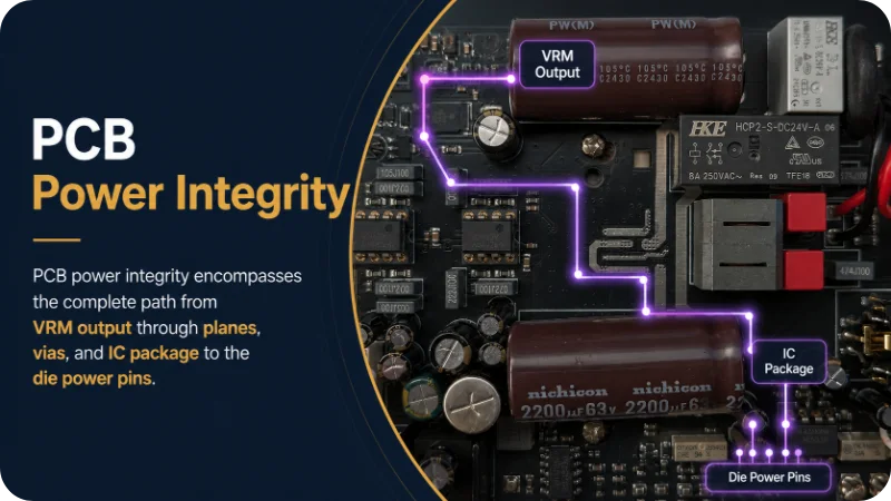
The power distribution network is the complete electrical path from the voltage regulator module (VRM) output through planes, vias, and package to the IC die. Every element in this path contributes impedance that must be controlled.
Target Impedance Calculation
Ztarget = Vripple_allowed / Ipeak
Example: 1.0 V rail · 3% ripple (30 mV) · 20 A peak → Ztarget = 1.5 mΩ
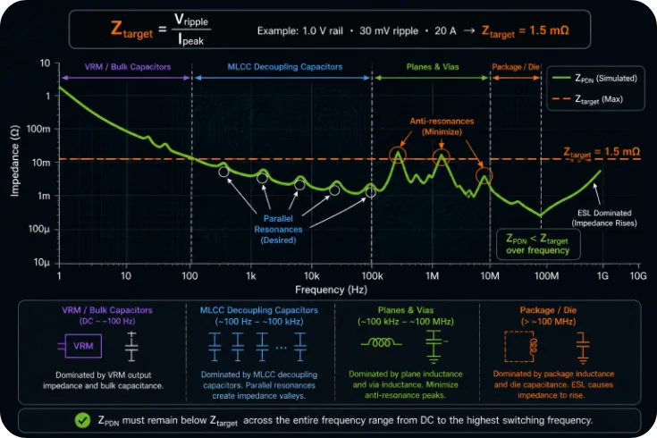
| Frequency Range | Controlling Element | Design Action |
|---|---|---|
| DC – 100 kHz | VRM output impedance + bulk capacitors | Select VRM loop bandwidth ≥ 200 kHz; size bulk capacitors to Cbulk = 1/(2π × fcrossover × Ztarget) |
| 100 kHz – 10 MHz | Ceramic MLCC decoupling capacitors | Place multiple MLCC values near IC power pins; minimize mounting inductance |
| 10 MHz – 1 GHz+ | PCB plane capacitance + package/die caps | Minimize GND-PWR plane separation; use 4 mil prepreg; consider embedded capacitance materials |
For complete PDN impedance analysis, VRM selection, bulk capacitor sizing, and PDN simulation methods, see our PCB power distribution network design guide.
VRM Placement Rules
- Place the VRM within 50 mm of the primary load IC
- Use wide, short copper connections from VRM output to the power plane — avoid routing through vias first
- Each via between VRM output and the plane adds approximately 0.5–1 nH inductance
- Position bulk capacitors between VRM and load, not only adjacent to the VRM output
3) Power Plane and Ground Plane Design
Plane design is the structural backbone of power integrity. Properly designed planes provide low-inductance current return paths, inherent distributed capacitance, and shielding for signal layers.

| Layer Count | Recommended Layer Order | PI Benefit |
|---|---|---|
| 4-layer | Signal / GND / PWR / Signal | GND-PWR coupling; ~150–380 pF/100 cm² plane capacitance with 4 mil prepreg |
| 6-layer | Signal / GND / Signal / PWR / GND / Signal | Dual GND references; PWR layer sandwiched between two GND planes |
| 8-layer | Signal / GND / Signal / PWR / GND / Signal / GND / Signal | All signal layers have immediate GND reference; lowest spreading inductance |
Core rule: always place a GND plane immediately adjacent to every PWR plane. The tight dielectric separation creates distributed capacitance providing high-frequency decoupling without discrete capacitors. For detailed 4, 6, 8, and 12-layer stackup configurations, see our multilayer PCB power and ground plane design guide.
Power Plane Split Rules
- Maintain at least 20 mil (0.5 mm) spacing between adjacent power plane splits
- Never route a high-speed signal across a plane split — the return current creates a radiating loop antenna
- Use a solid, unsplit GND plane as the reference for all signal layers when possible
- For unavoidable split crossings, place a 100 nF stitching capacitor directly at the crossing point
4) Decoupling Capacitor Strategy
Decoupling capacitors control mid-frequency PDN impedance by supplying instantaneous charge to ICs during switching events, preventing voltage droop on the power rail.
| Capacitor Type | Typical Value | Effective Frequency | Role |
|---|---|---|---|
| Bulk MLCC / polymer | 47–470 µF | DC – 500 kHz | Low-frequency energy reservoir, handoff from VRM |
| Large MLCC (0805) | 4.7–47 µF | 100 kHz – 5 MHz | Mid-frequency bulk decoupling |
| Standard MLCC (0402) | 100 nF – 1 µF | 1 MHz – 100 MHz | Primary local decoupling at IC power pins |
| Small MLCC (0201) | 1–100 nF | 50 MHz – 500 MHz | High-frequency decoupling, near BGA balls |
For detailed placement rules by IC package type (BGA, QFN, SOIC), via design configurations, and pad geometry optimization, see our PCB decoupling capacitor placement guide.
Placement Principles at a Glance
- Place the smallest (highest SRF) capacitors closest to IC power pins
- Use via-in-pad for capacitors targeting above 100 MHz — reduces Lmount by 0.5–2 nH
- Distribute capacitors around the full IC perimeter, not in a single line
- Use direct-connect pads (no thermal relief spokes) on power plane connections
5) Simultaneous Switching Noise (SSN) Control
Simultaneous switching noise (SSN) — also called ground bounce or delta-I noise — occurs when multiple output drivers switch at the same time. The aggregate current change (N × dI/dt) through the shared supply inductance generates voltage noise on both power and ground rails:
VSSN = Lsupply × N × (dI/dt)per output
Example: 32 outputs switching at 40 mA/ns with 1.3 nH supply inductance → VSSN ≈ 1.7 V peak
| Method | Mechanism | Typical SSN Reduction |
|---|---|---|
| Via-in-pad decoupling capacitors | Reduces Lmount by 0.5–2 nH per capacitor | 20–40% |
| Multiple parallel supply vias per BGA ball | Reduces effective via inductance in parallel | 15–30% |
| Programmable slow slew rate on I/O | Reduces dI/dt directly at the source | 40–67% |
| Separate VDDIO power domain from VDDC | Isolates I/O switching noise from core supply | 50–80% on core rail |
| Under-BGA 0201 decoupling capacitors | Minimises physical distance to supply ball | 25–45% |
For SSN calculation methodology, package inductance quantification, I/O domain isolation, and measurement techniques, see our PCB simultaneous switching noise reduction guide.
6) Power Integrity vs Signal Integrity: Key Interactions
Return Current Path Disruption
Every signal current has a return current flowing on the GND plane immediately below the signal trace. GND plane gaps, splits, or obstructing vias force the return current to detour around the obstruction, creating a large current loop. This degrades both PI (increased PDN inductance) and SI (increased EMI and crosstalk).
Power Rail Noise Coupling into Signal Circuits
Noise on the power rail couples into signal circuits through: (1) IC power supply rejection ratio (PSRR) limitations — every dB of headroom consumed by power noise appears on the IC’s signal output; (2) shared GND plane impedance — power rail current transients create voltage drops across GND plane resistance that appear as common-mode noise on signal traces.
Via Stitching for Reference Continuity
When signal layers transition between reference planes, stitching vias placed adjacent to the signal via maintain return path continuity and prevent impedance discontinuities. See our copper pour and via stitching guide for implementation details.
7) PCB Power Integrity Design Checklist Before Fabrication
This 7-step checklist addresses the most common PI failure modes identified during post-silicon debug. Complete all Critical steps before submitting Gerber files for fabrication.
| Step | Check Item | Requirement | Priority |
|---|---|---|---|
| 1 | Target impedance calculated | Ztarget defined for every power rail | Critical |
| 2 | VRM-to-load distance | < 50 mm for primary high-current load | Critical |
| 3 | GND plane adjacent to PWR plane | On every power layer pair | Critical |
| 4 | No high-speed signal crossing plane splits | Zero violations — DRC verified | Critical |
| 5 | Decoupling capacitor placement and value spread | ≥ 3 value decades; smallest cap nearest IC pin | High |
| 6 | Via stitching at all signal layer transitions | Stitching via within 1 mm of each transition via | High |
| 7 | Power plane copper coverage | > 70% fill; no isolated islands < 0.5 mm² | Medium |
8) Frequently Asked Questions
What is the difference between power integrity and signal integrity in PCB design?
Signal integrity (SI) focuses on the quality of data signals transmitted between components — measuring eye diagram opening, jitter, and crosstalk on I/O traces. Power integrity (PI) focuses on the quality of the DC supply voltage delivered to component power pins — measuring PDN impedance, voltage droop, and ripple. Both disciplines interact and must be designed together for reliable high-speed PCB operation.
What is target impedance and how do I calculate it?
Target impedance is the maximum allowable PDN impedance at any frequency to keep power rail noise within budget. Calculate it as: Ztarget = Vripple_allowed / Ipeak. For a 1.0 V rail with 3% ripple (30 mV) and 20 A peak current: Ztarget = 1.5 mΩ. This target must be maintained flat from DC through the bandwidth of the fastest switching transient — often several hundred MHz for modern processors.
How many decoupling capacitors do I need per IC?
Calculate Ztarget for each power rail, then select capacitor types and quantities to maintain impedance below that target across the full frequency range. Always use at least 3 capacitor value decades per rail (e.g., 10 µF, 100 nF, 10 nF) to avoid impedance gaps between frequency regions. As a starting point: one 100 nF and one 10 nF 0402 MLCC per power pin pair, validated with PDN simulation.
Does a 4-layer PCB provide adequate power integrity for DDR4 memory?
Yes, with careful design. A 4-layer board (Signal / GND / PWR / Signal) can support DDR4 at 3200 MT/s if GND-PWR plane spacing is 4 mil or less, adequate decoupling is within 5 mm of DRAM power pins, and the VRM is close to the memory array. DDR5 generally benefits from 6-layer or higher stackups due to tighter PDN impedance targets.
Can via-in-pad improve power integrity for decoupling capacitors?
Yes. Via-in-pad eliminates trace stub inductance between the capacitor pad and the via, reducing mounting inductance by 0.5–2 nH. A 100 nF 0402 MLCC achieves SRF of 65–90 MHz with via-in-pad versus 40–65 MHz with adjacent-via placement. Via-in-pad adds approximately 15–25% to PCB fabrication cost and requires filled, planarized vias. See our via-in-pad guide for manufacturing requirements.
Highleap Electronics supports PCB power integrity design from stackup selection through fabrication. Our engineering team provides free PDN design reviews for qualified projects, identifying power integrity issues before fabrication. Contact us to discuss your high-speed PCB requirements.

Recommended Posts

Custom Rogers RO4835 PCB Fabrication & Assembly Services
Figure 1. Rogers RO4835 PCBRogers RO4835 PCB is a...

Nelco N4000-13 PCB Material and Manufacturing Guide | Highleap Electronics
Figure 1. Nelco N4000-13 PCBNelco N4000-13 PCB is a...

Rogers RT/duroid 6002 PCB Manufacturer — Specifications, Stackup, Quote
Figure 1. Rogers RT/duroid 6002Rogers RT/duroid 6002 is...

Miniaturize Antennas with Rogers TMM Laminates
Figure 1. Rogers TMM Executive Summary: Rogers TMM...
How to get a quote for PCBs
Let us run DFM/DFA analysis for you and get back to you with a report.
You can upload your files securely through our website.
We require the following information in order to give you a quote:
-
- Gerber, ODB++, or .pcb, spec.
- BOM list if you require assembly
- Quantity
- Turn time