
TMM PCB for Antenna Miniaturization
The antenna-miniaturization page is intentionally narrower than the TMM family manufacturing page. It focuses on how dielectric construction and finished thickness change antenna dimensions, while keeping feed geometry, ground structure and fabrication tolerance tied to the released antenna design.
Figure 1. Rogers TMM
TMM constructions can reduce some antenna feature dimensions when the selected grade provides a higher dielectric constant, but the finished antenna still depends on dielectric thickness, copper geometry, feed transition, ground structure and fabrication tolerance. Material scope: the Rogers product name is used to identify the laminate specified for the PCB build. Highleap Electronics provides PCB fabrication and assembly, while the laminate is sourced and verified separately. Executive Summary: This page focuses on using the TMM family in antenna miniaturization projects, with grade selection tied to the required electrical construction and manufacturing window. Current supplier documentation should be used for the specified grade, thickness and foil construction rather than treating family-level values as a substitute for a released stackup.
Table of Contents
- What Is Rogers TMM Laminate Material
- Rogers TMM Series Properties Table (TMM3–TMM13i) — Reference Values and Design Use
- TMM3 and TMM4: Low-Dk for Filters, Oscillators, and Calibration Substrates
- TMM6 and TMM10: High-Dk for GPS Antennas and Base Station Arrays
- TMM10i and TMM13i: Highest-Dk Rogers Laminates for Miniaturized Antennas
- How to Manufacture TMM PCBs: Drilling, Plating, and Lamination
- Rogers TMM vs RO4000 vs RO3000: Material Selection Guide
1. TMM Grade Selection for Antenna Miniaturization
TMM is a family of thermoset microwave laminates used in microstrip and stripline constructions. For antenna work, the useful manufacturing question is which grade and thickness provide the required electrical geometry while remaining compatible with the intended drilling, routing, lamination and plating route. Rogers publishes separate fabrication guidance for the TMM family, so the released construction should be checked against the current supplier documentation before tooling. The PCB manufacturing process should then be matched to that construction.
For antenna miniaturization, the relevant variables are grade-specific Dk, dielectric thickness, copper construction, temperature behavior and the relationship between the RF feature size and manufacturing tolerance. These values should be taken from the current supplier datasheet for the selected grade rather than generalized across all TMM products. Highleap reviews antenna feeds, reference-plane spacing, line width and board thickness against the modeled construction. As dimensions shrink, panel registration and etch control become more important, so the first article should measure the features that drive the antenna response. Exact material property values should be checked against the current supplier documentation for the specified grade and construction.
Because TMM is thermoset, it does not soften when heated. Wire bonding can be performed without risk of pad lifting or substrate deformation — a significant advantage over PTFE for hybrid microwave integrated circuits (MICs).
2. Rogers TMM Series Properties Table (TMM3–TMM13i) — Reference Values and Design Use
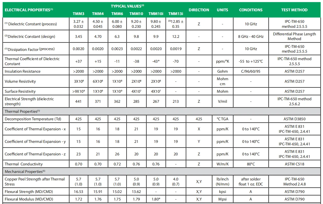
The values below are reference data from published Rogers TMM technical literature; verify the current revision and test method before release. “Process Dk” is measured at 10 GHz per IPC-TM-650 method 2.5.5.5 (stripline resonator, z-axis). “Design Dk” is the broadband value measured 8–40 GHz by differential phase length method — use the Design Dk in your EM simulation (HFSS, ADS, CST).
| Property | TMM3 | TMM4 | TMM6 | TMM10 | TMM10i | TMM13i | Conditions / Method |
|---|---|---|---|---|---|---|---|
| Dk (process) @ 10 GHz | 3.27 ± 0.032 | 4.50 ± 0.045 | 6.00 ± 0.080 | 9.20 ± 0.230 | 9.80 ± 0.245 | 12.85 ± 0.35 | z-axis, IPC-TM-650 2.5.5.5 |
| Dk (design) 8–40 GHz | 3.45 | 4.70 | 6.30 | 9.80 | 9.90 | 12.20 | Differential phase length |
| Df @ 10 GHz | 0.0020 | 0.0020 | 0.0023 | 0.0022 | 0.0020 | 0.0019 | z-axis, IPC-TM-650 2.5.5.5 |
| TCDk (ppm/°K) | +37 | +15 | −11 | −38 | −43* | −70 | −55 to +125 °C |
| CTE x,y (ppm/°K) | 15 | 16 | 18 | 21 | 19 | 19 | 0–140 °C, ASTM E831 |
| CTE z (ppm/°K) | 23 | 21 | 26 | 20 | 20 | 20 | 0–140 °C, ASTM E831 |
| Thermal conductivity (W/m·K) | 0.70 | 0.70 | 0.72 | 0.76 | 0.76 | — | z-axis, 80 °C, ASTM C518 |
| Specific gravity | 1.78 | 2.07 | 2.37 | 2.77 | 2.77 | 3.00 | ASTM D792 |
| Copper peel (lb/in) | 5.7 | 5.7 | 5.7 | 5.0 | 5.0 | 4.0 | After solder float, 1 oz ED copper |
| Td (°C) | 425 | 425 | 425 | 425 | 425 | 425 | TGA, ASTM D3850 |
| Lead-free compatible | Yes | Yes | Yes | Yes | Yes | Yes | — |
* TMM10i TCDk is estimated per Rogers datasheet. TMM13i thermal conductivity not published. Water absorption varies by substrate thickness — see Rogers datasheet for thickness-specific values (ASTM D570). Standard thicknesses: 0.015″–0.500″ (15–500 mil). Standard panel sizes: 18 × 12″ and 18 × 24″. Copper cladding: ½ oz, 1 oz, 2 oz electrodeposited; heavy metal cladding available.
Key data patterns: Df stays low (0.0019–0.0023) across all variants regardless of Dk — designers can select high Dk for miniaturization without a significant loss penalty. CTE x-y and CTE z are close in every variant (unlike FR4, where z-CTE is 3–5× higher than x-y), which is the foundation for reliable plated through-holes.
Process Dk vs Design Dk: The two values differ because they are measured by different methods at different frequency ranges. For example, TMM4 has process Dk = 4.50 but design Dk = 4.70. Use process Dk only for manufacturing quality control. Note that TMM13i’s design Dk (12.20) is lower than its process Dk (12.85) — always verify which value your simulation tool expects.
3. TMM3 and TMM4: Low-Dk for Filters, Oscillators, and Calibration Substrates
TMM3 (Dk = 3.27 process / 3.45 design). TMM3 is closest to RO4350B in dielectric constant. Its TCDk of +37 ppm/°K means the dielectric constant increases slightly with temperature — a predictable, well-characterized drift that can be compensated in design. Over the −55 to +125 °C military temperature range, total Dk shift is approximately 0.7 %, keeping filter center frequencies stable without post-manufacturing tuning. TMM3 is used in satellite transponder filters, voltage-controlled oscillator (VCO) substrates, and test fixtures where Dk must be known to high accuracy and repeatable across production lots.
TMM4 (Dk = 4.50 process / 4.70 design). TMM4 has the smallest TCDk magnitude in the entire TMM family: +15 ppm/°K. Over −55 to +125 °C, total Dk drift is approximately 0.27 % — the most temperature-stable option in the Rogers portfolio. Its design Dk of 4.70 is close to FR4 (4.2–4.5), so designs prototyped on FR4 can transition to TMM4 without changing circuit dimensions. TMM4 is the standard choice for combline and interdigital filters in communication systems and military radios where frequency accuracy must hold stable from −55 to +125 °C.
4. TMM6 and TMM10: High-Dk for GPS Antennas and Base Station Arrays
Higher Dk reduces the guided wavelength, proportionally shrinking resonant structures. A patch antenna on TMM6 (Dk = 6.00) is approximately 35 % smaller per dimension than the same antenna on TMM3 (Dk = 3.27). On TMM10 (Dk = 9.20), the size reduction reaches approximately 50 %.
TMM6 (Dk = 6.00 process / 6.30 design). TMM6 is the most widely used TMM variant. GPS L1 (1.575 GHz) patch antennas on TMM6 achieve a footprint of roughly 25 × 25 mm — compact enough for automotive roof modules and handheld receivers. The TCDk of −11 ppm/°K (the only negative-and-small TCDk in the family) can be a strong candidate when both miniaturization and temperature stability are required. TMM6 is also the standard material for cellular base station sector antenna panels, where 35 % size reduction per element allows more radiators in a fixed panel area for 5G massive-MIMO arrays.
TMM10 (Dk = 9.20 process / 9.80 design). TMM10 pushes miniaturization further — a 50 % size reduction versus TMM3. Applications include dielectric resonator antenna (DRA) designs and compact arrays for Wi-Fi and 5G. TMM10 and TMM10i can replace alumina ceramic substrates while remaining processable on standard PCB equipment — Rogers specifically notes this capability in the TMM datasheet. Trade-off: CTE x-y increases to 21 ppm/°K and the material becomes more brittle at higher ceramic loading.
5. TMM10i and TMM13i: Highest-Dk Rogers Laminates for Miniaturized Antennas
The “i” suffix designates isotropic-CTE variants. TMM10i (Dk = 9.80) and TMM13i (Dk = 12.85) have CTE closely matched in all three axes: both measure 19/19/20 ppm/°K (x/y/z) — the most consistent thermal expansion of any Rogers laminate.
TMM10i (Dk = 9.80 process / 9.90 design). TMM10i is preferred over TMM10 for high-reliability programs. Its specific gravity (2.77) is identical to TMM10, but the more isotropic CTE (19/20 vs TMM10’s 21/20) reduces differential stress between copper via barrels and surrounding dielectric during thermal cycling. Applications include phased-array antenna elements for aerospace radar, dielectric-loaded cavity filters for communication satellites, and power divider networks where PTH reliability over 1,000+ thermal cycles is non-negotiable.
TMM13i (Dk = 12.85 process / 12.20 design). TMM13i provides the most aggressive miniaturization in the Rogers portfolio — antenna elements are approximately 60 % smaller per dimension than on TMM3. It is a niche material for ultra-compact GNSS antennas, miniaturized ceramic patch arrays, and dielectric resonator oscillators (DROs). Trade-offs: highest density (3.00 g/cm³), TCDk of −70 ppm/°K (largest temperature drift in the TMM family), lower copper peel strength (4.0 lb/in vs 5.7 for TMM3), and thermal conductivity not published by Rogers. When maximum Dk with thermoset processability is required, TMM13i is the only laminate option short of custom ceramic substrates.
6. How to Manufacture TMM PCBs: Drilling, Plating, and Lamination
TMM’s thermoset matrix means it processes on standard FR4 equipment — a major advantage over PTFE. The ceramic filler introduces specific adjustments, and brittleness increases with Dk.
| Process Step | FR4 Baseline | TMM Adjustment |
|---|---|---|
| Lamination temperature | 175–185 °C | Same — thermoset cure at standard FR4 temperatures |
| Drilling — bit life | 1,000+ hits | TMM3/4/6: 500–700 hits. TMM10/10i/13i: 300–500 hits |
| Drilling — feed rate | Standard | Reduce 20 % for all TMM variants |
| Desmear | Permanganate | Standard permanganate — no plasma or sodium etch needed |
| Copper peel strength | > 6 lb/in | 5.0–5.7 lb/in (TMM3–TMM10i); 4.0 lb/in (TMM13i) |
| Hybrid builds | N/A | Compatible with FR4 prepreg and other TMM variants |
| Depaneling | Routing or V-score | V-score preferred for high-Dk variants — brittle material depanels cleaner |
| Wire bonding | Not recommended | Supported — thermoset does not soften under bonding heat |
For TMM10, TMM10i, and TMM13i, laser drilling is recommended for microvias — the brittle material can micro-crack around small mechanically drilled holes. Design minimum trace width at 4 mil for TMM3/TMM4/TMM6 and 5 mil for TMM10/TMM10i/TMM13i. Include impedance test coupons on every panel.
Highleap manufactures TMM PCBs across all six variants. TMM3, TMM6, and TMM10i are stocked in standard thicknesses (25 and 50 mil). TMM4, TMM10, and TMM13i are available on order with 2–4 week material lead time. Multilayer TMM constructions up to 8 layers and TMM/FR4 hybrid stackups are supported. For the complete fabrication process covering all Rogers material families, see the Rogers PCB fabrication process guide.
7. Rogers TMM vs RO4000 vs RO3000: Material Selection Guide
| Design Requirement | Candidate | Why |
|---|---|---|
| Lowest loss (Df < 0.001) | RT/duroid 5880 | PTFE base gives Df = 0.0009; TMM Df ≈ 0.002 is 2× higher |
| Cost/performance candidate for general RF 1–30 GHz | RO4350B / RO4003C | Lower cost, similar Dk range, more widely stocked |
| Dk temperature-stability candidate | TMM4 (TCDk = +15 ppm/°K) | Lowest TCDk magnitude in any Rogers family |
| High Dk for miniaturization (Dk > 6) | TMM6 / TMM10 / TMM10i / TMM13i | Only thermoset family offering Dk up to 12.85 |
| Alumina ceramic substrate replacement | TMM10 / TMM10i | Similar Dk to alumina, processable as standard PCB |
| Isotropic CTE for via reliability | TMM10i / TMM13i | x-y-z CTE matched closest to copper |
| Easy hybrid with FR4 | RO4000 or TMM3/TMM4 | Both thermoset, same press cycle as FR4 |
| Millimeter-wave > 40 GHz | RO3003 / RT/duroid | PTFE loss lower than TMM at mmWave frequencies |
The clearest use case for TMM is when a design needs Dk above 6.0 combined with standard PCB processability — no other Rogers series offers this in a thermoset format. The second strong use case is temperature-stable phase performance: TMM4’s TCDk of +15 ppm/°K is the lowest magnitude in the Rogers portfolio, making it the standard for narrowband satellite communication filters and precision radar feed networks where frequency stability across −55 to +125 °C is critical.
TMM is not the right choice when absolute minimum insertion loss is required (use RT/duroid 5880), when operating primarily above 40 GHz (PTFE outperforms TMM at mmWave), or when cost is the primary driver for general RF below 10 GHz (RO4350B is cheaper and more widely stocked).
Request a TMM PCB quote from Highleap → Submit Gerber files and stackup requirements. Engineering consultation on TMM vs RO4000 vs RO3000 trade-offs included at no charge. For a miniaturized antenna quote, provide the frequency band, antenna geometry, stackup, board outline, copper and RF test requirement. This lets the manufacturer assess whether the required feature size is compatible with the proposed build.

Recommended Posts

TMM4 Filter PCB Manufacturing
TMM4 filter PCB manufacturing is controlled by the...

TMM3 PCB Manufacturing for RF Modules
TMM3 PCB manufacturing is most useful where the RF module...

TMM6 PCB Fabrication
TMM6 fabrication is the process-control page for a mid-Dk...

TMM10 PCB Manufacturing for Compact RF Designs
Table of contentsHow TMM10 Shrinks RF StructuresTMM10 vs...
How to get a quote for PCBs
Let’s run DFM/DFA analysis for you and get back to you with a report. You can upload your files securely through our website. We require the following information in order to give you a quote:
-
- Gerber, ODB++, or .pcb, spec.
- BOM list if you require assembly
- Quantity
- Turn time
For PCBA services, please provide your BOM (Bill of Materials) and any specific assembly instructions. We also offer DFM/DFA analysis to optimize your designs for manufacturability and assembly, ensuring a smooth production process.