
Server Motherboard PCB Manufacturing and Assembly
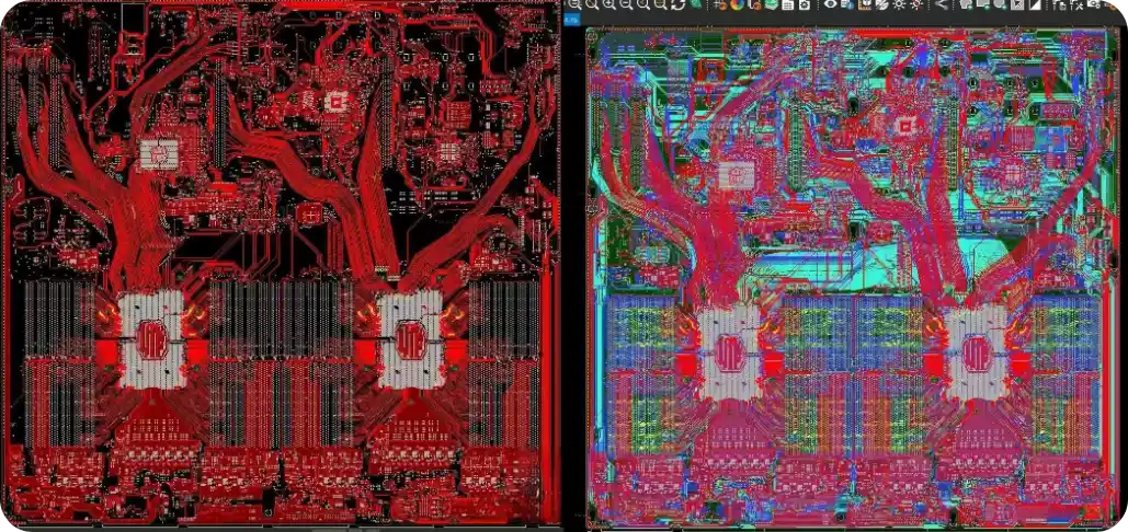
Server motherboard PCB manufacturing is becoming more demanding as data centers, AI computing, cloud infrastructure and high-performance storage systems require greater processing capability and higher data bandwidth. The motherboard has to connect processors, memory, storage, networking and expansion interfaces while also supporting complex power delivery, thermal management and high-speed signal transmission.
At the same time, the manufacturing environment in 2026 is different from a few years ago. PCB laminate, copper-related materials and other manufacturing inputs are subject to price changes, while memory, storage and other electronic components are also experiencing supply and pricing pressure as AI and data-center demand continues to grow. For a server motherboard project, the manufacturing decision therefore involves more than selecting a PCB supplier and comparing a bare-board price.
The right approach also depends on the project stage. A prototype motherboard that still requires electrical, thermal and system validation should be managed differently from a design that has already been released for mass production. For prototypes, product iteration and engineering validation can be more important than minimizing the first PCB build cost. For volume production, PCB material cost, component availability, BOM cost, production capacity and purchasing timing become much more significant.
Highleap Electronics manufactures complex multilayer PCBs and provides PCB assembly for demanding electronic applications. Server motherboard projects can be reviewed according to the actual PCB construction, material requirements, high-speed design requirements, assembly data, production quantity and schedule.
Planning a server motherboard PCB project? Send the available PCB files and production requirements through the PCB Quote page for engineering and manufacturing review.
Server Motherboard PCB Manufacturing in 2026
Server motherboard manufacturing in 2026 is being influenced by both technology requirements and supply-chain conditions. AI infrastructure and data-center expansion are increasing demand for high-performance computing hardware, while PCB manufacturers and component suppliers are dealing with changes in material costs, capacity allocation and lead times.
Memory is one of the clearest examples. TrendForce reported that conventional DRAM contract prices were expected to rise 55–60% quarter over quarter in the first quarter of 2026, while NAND Flash prices were expected to rise 33–38%. Its third-quarter 2026 outlook still projected further increases of 13–18% for conventional DRAM and 10–15% for NAND Flash, with AI server and data-center demand continuing to support the market. :contentReference[oaicite:3]{index=3}
The supply situation is also closely connected to HBM and server demand. Samsung said in September 2026 that HBM could account for nearly 30% of global DRAM wafer capacity in 2027, compared with about 20% currently, illustrating how AI-related memory demand can affect the broader DRAM supply structure. :contentReference[oaicite:4]{index=4}
PCB fabrication is facing its own cost pressure. CCL, FR-4, high-Tg and high-speed materials can be affected by resin, glass fiber and copper-related costs, while high-layer-count and HDI boards can be more sensitive to changes in material pricing because they consume more complex laminate and fabrication resources. Industry reports in 2026 have also documented CCL and FR-4 price adjustment signals. :contentReference[oaicite:5]{index=5}
These conditions do not mean that every server motherboard should be purchased immediately or that every project should wait. The more useful approach is to distinguish between prototype development, NPI, low-volume production and established mass production, because each stage has a different cost and supply priority.
| Project Stage | Main Objective | Cost and Supply Priority |
|---|---|---|
| Prototype | Hardware validation and product iteration | Control unnecessary cost without delaying development |
| NPI | Design and manufacturing validation | Balance engineering changes, BOM and manufacturing stability |
| Low Volume | Stable initial production | Evaluate PCB, component and assembly costs together |
| Mass Production | Repeatable production and supply continuity | Plan material, components, capacity, cost and schedule together |
Server Motherboard vs Standard Motherboard PCB
Server and desktop motherboards perform the same fundamental function of connecting processors, memory and peripheral devices, but the manufacturing requirements can be substantially different. A server motherboard may need to accommodate multiple processor or accelerator connections, large numbers of memory channels, high-speed PCIe links, storage interfaces, networking hardware, management controllers and complex power-delivery circuits on the same PCB.
The result is a PCB with much greater routing density and more demanding electrical and mechanical requirements. The board may require additional routing layers, controlled-impedance structures, advanced via technology and materials selected for high-speed transmission. These requirements also make manufacturing tolerances and process control more important.
| Design Area | Standard Motherboard | Server Motherboard |
|---|---|---|
| Routing Density | Moderate to high | Very high for processors, memory and expansion interfaces |
| Layer Structure | Multilayer PCB | High-density multilayer construction |
| High-Speed Interfaces | Several high-speed interfaces | Multiple high-speed memory, PCIe, networking and storage connections |
| Via Technology | Conventional vias are common | Blind, buried, microvia and backdrilling structures may be required |
| Material | Often conventional PCB materials | Material may be selected according to signal-loss and reliability requirements |
| Power Distribution | Multiple power rails | High-density power delivery and thermal structures |
A typical server motherboard may place processors near large banks of memory while routing high-speed links toward PCIe slots, storage interfaces and networking connections. This physical arrangement creates thousands of interconnections that must pass through the available PCB layers without compromising reference planes, impedance or power distribution.
For the PCB manufacturer, this means that server motherboard fabrication cannot be evaluated only from the external board dimensions. The complete stackup, material system, copper structure, via technology, impedance requirements and mechanical design all need to be considered together.
Server Motherboard PCB Materials
Material selection becomes increasingly important as the data rate of a server motherboard increases. A PCB transmission path experiences both conductor loss and dielectric loss, and the total loss of a high-speed channel depends on the material, copper structure, trace geometry and signal frequency.
For lower-speed portions of a design, a suitable FR-4 system may be sufficient. Higher-speed interfaces can require materials with lower dielectric loss and more controlled electrical characteristics. The appropriate material should therefore be selected from the actual signal-integrity requirements rather than from the general label of “server PCB.”
Important material parameters can include:
- Dielectric constant (Dk)
- Dissipation factor (Df)
- Insertion-loss characteristics
- Thermal performance
- Coefficient of thermal expansion
- Glass construction
- Resin system
- Copper foil profile
- Core and prepreg thickness
For high-speed designs, lower-loss laminate systems and low-profile copper structures may be selected to reduce signal attenuation. The choice is not simply a matter of selecting the material with the lowest Df; the complete stackup, routing geometry, copper profile, fabrication process and required signal performance have to be considered together.
Material availability is also becoming a procurement consideration in 2026. A material selected for a prototype may not necessarily have the same price or lead time when the project enters mass production. For production programs, it is therefore useful to confirm material availability and procurement conditions before the final production schedule is released.
Highleap Electronics manufactures finished PCBs using customer-specified materials and does not manufacture PCB laminates. If a server motherboard uses a particular high-speed or low-loss laminate, the material model should be included in the manufacturing documentation so that the quotation and fabrication process are based on the actual requirement.
For projects where material electrical performance and controlled impedance are important, see High-Frequency PCB Manufacturing.
Server Motherboard Layer Stackup and Manufacturing Challenges
The layer stackup provides the physical foundation for the electrical design. Signal layers, power planes and ground planes need to be arranged so that high-speed routes have suitable reference structures while the board also provides enough routing capacity for memory, processor, storage and expansion interfaces.
Increasing the layer count provides more routing resources, but it also makes fabrication more demanding. As more layers are combined into a multilayer structure, layer registration, lamination, drilling, plating and dimensional stability become increasingly important. A manufacturing problem on an internal layer can remain hidden after lamination, making process control essential.
Important stackup and fabrication parameters include:
- Total layer count
- Signal layer assignment
- Ground and power plane locations
- Core and prepreg thickness
- Individual layer copper thickness
- Finished board thickness
- Impedance-controlled structures
- Via transitions
- Blind and buried vias
- Laser microvias
- Backdrilling where required
Drilling becomes particularly important when a thick multilayer board contains small holes. The relationship between finished board thickness and hole diameter determines the aspect ratio, which affects the difficulty of producing reliable plated holes.
Backdrilling can be used when through-hole vias extend beyond the layers required by a high-speed signal. The unused section of the via can behave as a stub and introduce unwanted electrical discontinuities. When backdrilling is specified, the manufacturing drawing needs to clearly define the required structure and depth limits.
HDI construction introduces another level of complexity because laser-drilled microvias have to connect accurately to their target structures. Depending on the released design, stacked or staggered microvias, via-in-pad structures and sequential lamination may be required.
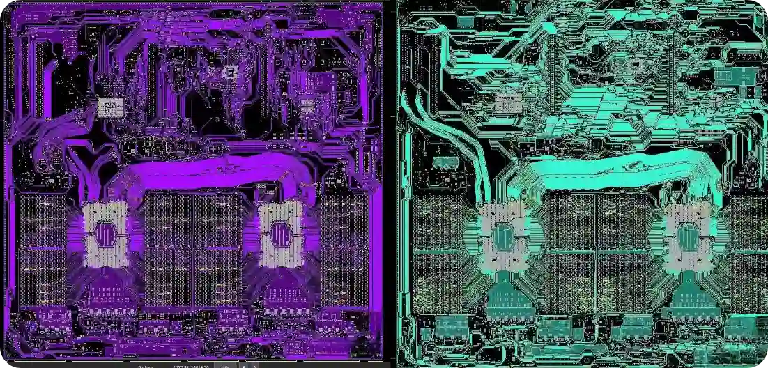
The key manufacturing issue is not simply producing more layers. It is maintaining the electrical and mechanical relationships defined by the released stackup throughout fabrication.
High-Speed Signal Integrity and Routing
High-speed interfaces are one of the defining characteristics of modern server motherboards. PCIe, high-speed memory, networking and storage interfaces all depend on transmission paths whose electrical characteristics are controlled by the PCB structure.
At high data rates, a PCB trace cannot be treated as an ideal wire. Trace width, copper thickness, dielectric height, material properties, reference-plane position, differential-pair spacing and via transitions all contribute to the behavior of the channel.
PCB manufacturing parameters affecting high-speed performance include:
- Trace width and spacing
- Copper thickness
- Dielectric thickness
- Material Dk and Df
- Reference-plane location
- Differential-pair geometry
- Via structure
- Via stub length
- Backdrill depth
- Etching accuracy
Controlled impedance therefore has to be linked to the actual stackup. If the dielectric thickness or copper structure changes, the trace geometry required for the target impedance can also change. This is why a manufacturer should not substitute a different stackup simply because the PCB still has the same number of layers.
High-speed channels are also affected by insertion loss, return loss, crosstalk and discontinuities at vias and connectors. These are established primarily during PCB design, but the manufacturer has to reproduce the physical structure on which the electrical design was based.
For very high-speed interfaces, material selection and copper surface characteristics can become increasingly important. The appropriate solution depends on the channel length, data rate, loss budget, stackup and device requirements of the specific server platform.
Highleap Electronics manufactures high-frequency and high-speed PCBs according to customer-specified material, stackup and fabrication requirements.
Power Delivery and Thermal Management
Server motherboard power delivery is closely connected to PCB construction. Processors, memory and accelerator-related hardware can require multiple power rails and substantial current, while the same board has to maintain signal integrity across high-speed interfaces.
The PCB contributes to power delivery through power planes, ground structures, copper areas and via arrays. It also contributes to thermal management by providing conductive paths through copper layers and thermal vias.
Important PCB structures can include:
- Power and ground planes
- High-current copper areas
- Power distribution layers
- Thermal via arrays
- Via structures beneath power components
- Large copper regions
- Ground structures around high-speed and power devices
Heavier copper can provide greater current-carrying capability and help distribute heat, but it also changes the fabrication process. Large copper areas and different copper weights across layers can affect etching, plating, lamination and dimensional stability.
Thermal vias can transfer heat from surface components into internal copper structures. The final thermal performance, however, depends on the complete system, including component power, heatsinks, airflow, mechanical design and the PCB construction. The PCB should therefore be considered one part of the thermal solution rather than a standalone heat sink.
Thermal reliability is also affected by the different expansion characteristics of copper, resin and laminate. Repeated heating and cooling can place stress on plated holes, vias and multilayer structures, making material selection and fabrication quality important for long-term reliability.
Server PCB Quality and Reliability
A server motherboard is expected to operate as part of a continuously running computing system, so PCB quality cannot be evaluated only by whether the outer-layer artwork looks correct. Internal layer connections, plated holes, microvias, impedance structures and board dimensions all need to remain within the released manufacturing requirements.
For complex multilayer boards, quality control starts with the manufacturing data. CAM review can identify potential fabrication issues before production, while inspection during inner-layer processing can detect circuit defects before the layers are permanently laminated together.
Depending on the project requirements, inspection can include:
- AOI for circuit-pattern inspection
- Electrical testing for opens and shorts
- Dimensional inspection
- Visual inspection
- Impedance verification
- X-ray inspection where applicable
For high-speed designs, impedance verification can provide manufacturing feedback on controlled-impedance structures. For assembled boards containing BGA packages, X-ray inspection can be used to examine solder joints that are hidden beneath the component body.
Additional reliability testing may be required when specified by the customer or product standard. The appropriate testing program should be determined from the actual PCB construction, application requirements and quality specification rather than assuming that every server motherboard needs the same test package.
For a production server motherboard, the most important objective is repeatability. The manufacturer needs to reproduce the released construction consistently across production batches, especially when the board contains high layer counts, HDI structures, high-speed routing and complex copper distribution.
Prototype vs Mass Production Server PCB
One of the most important decisions for a server motherboard project is determining how much attention should be given to PCB cost at each stage of development. A prototype and a mass-production board may use the same basic design, but the purchasing priorities are different.
Prototype Server Motherboard PCB
For a prototype, the main objective is to validate the product. The engineering team may need to verify processor operation, memory stability, PCIe links, storage, networking, power sequencing, thermal behavior, firmware and mechanical integration. The first PCB revision may also reveal problems that require changes to routing, component placement or power delivery.
For this reason, a prototype should generally prioritize product iteration, manufacturing consistency and reasonable lead time rather than focusing exclusively on the lowest PCB unit price. If only a small number of boards are being built, the financial difference between two PCB quotations may be much smaller than the cost of delaying the next engineering revision.
2026 price volatility makes this distinction even more relevant. Waiting for a lower material or component price can be reasonable when the project schedule is genuinely flexible, but it should not become a reason to delay an important engineering validation build when the product still needs to be tested.
For prototype projects, a practical priority is:
- Build the current engineering revision.
- Validate electrical and thermal performance.
- Identify design or manufacturing issues.
- Update the PCB and BOM.
- Build the next revision when necessary.
- Optimize production cost after the design becomes stable.
Mass Production Server Motherboard PCB
Mass production is different because PCB and component costs are multiplied across the production quantity. A small change in PCB material cost, memory pricing or another critical BOM item can have a substantial effect when the project involves thousands of assembled boards.
For a confirmed production program, it is therefore useful to review PCB material availability, component supply, quotation validity, manufacturing capacity and the required delivery schedule together. Waiting for a lower price should not be treated as a guaranteed strategy because PCB materials and electronic components can become more expensive as well as cheaper.
When the production schedule is flexible, the purchasing team can compare different purchasing windows and approved component or material options. When the production schedule is already committed, the priority is usually to secure the required supply at an acceptable total cost without creating a production delay.
For mass production, evaluate the total manufacturing cost rather than the bare PCB price alone. The relevant calculation can include PCB fabrication, components, assembly, testing, yield, logistics and the cost of delayed production.
| Consideration | Prototype | Mass Production |
|---|---|---|
| PCB Unit Price | Important but usually secondary to iteration | Major cost factor at production volume |
| Material Planning | Meet the current prototype requirement | Consider availability, price and production continuity |
| Components | Small quantity and engineering validation | Supply, pricing and approved alternatives become critical |
| Production Timing | Support the next engineering revision | Coordinate with the production schedule |
| Main Objective | Validate and improve the product | Control total cost and maintain supply |
Server Motherboard PCB Assembly
For a complete server motherboard project, PCB fabrication is only one part of the manufacturing process. The assembled PCBA can contain processors, memory devices, BGA packages, fine-pitch components, power-management devices, connectors and other components whose cost and availability may have a greater impact on the total product cost than the bare PCB itself.
Component sourcing should therefore be considered together with PCB fabrication and assembly. A BOM that is suitable for a prototype may need to be reviewed again before mass production because component availability, pricing, lifecycle status or approved alternatives can change during the development cycle.
A typical server motherboard PCBA package includes:
- Bill of Materials
- Manufacturer part numbers where applicable
- Pick-and-Place data
- Assembly drawings
- Component orientation information
- BGA and fine-pitch component requirements
- Special assembly instructions
- Inspection requirements
- Electrical or functional testing requirements
BGA assembly requires particular attention because the solder joints are hidden underneath the package. PCB pad geometry, solder mask, surface finish, via structures and board flatness can therefore affect assembly quality. For server motherboards with dense BGA areas, PCB fabrication and PCBA should be planned together rather than treating the two processes as completely independent.
Highleap Electronics provides PCB Assembly together with PCB fabrication. Depending on the project requirements, assembly can include SMT, through-hole and BGA assembly, with inspection and testing according to the customer’s requirements.
For projects requiring PCB fabrication, component sourcing and assembly through one manufacturing workflow, see Turnkey PCB Assembly.
Server Motherboard PCB Quote
The information required for a server motherboard quotation depends on whether the project requires bare PCB fabrication, PCB assembly or both. Providing the actual manufacturing data allows the supplier to evaluate the construction rather than estimating the price from board dimensions and layer count alone.
For PCB fabrication, provide:
- Gerber files or equivalent fabrication data
- NC Drill files
- PCB fabrication drawing
- Layer stackup
- Material specification
- Finished board thickness
- Copper requirements
- Surface finish
- Controlled impedance requirements
- HDI requirements
- Blind and buried via requirements
- Microvia requirements
- Backdrilling requirements
- PCB quantity
For PCBA, also provide:
- BOM
- Pick-and-Place files
- Assembly drawing
- Component specifications
- Testing requirements
- Required quantity
- Target production schedule
For a prototype project, the available engineering data can be submitted even if the final production package is still being completed. An early manufacturing review can help identify PCB construction issues and provide an initial cost and lead-time reference before the next engineering build.
For mass production, it is useful to provide the expected production quantity and target schedule together with the PCB and BOM data. This allows the quotation to be evaluated in the context of material requirements, component sourcing, PCB production and assembly capacity.
2026 pricing conditions can change, so a quotation should also be reviewed for validity period, material availability and component availability before a large production order is released.
For server motherboard projects that are still in development, the priority may be to obtain a manufacturable prototype quickly and continue product validation. For confirmed production programs, the focus can shift toward securing the required PCB materials and components, controlling total manufacturing cost and maintaining the production schedule.
Request a Server Motherboard PCB Manufacturing and Assembly Quote

Recommended Posts

5G Small Cell PCB Manufacturing for RF and Telecom Infrastructure
Table of Contents 5G Small Cell PCB Requirements Depend on...
Custom 65% Keyboard PCB and PCBA Manufacturing
Table of contents 1. From Design Files to Production-Ready...
RFSoC Board PCB Manufacturing and Assembly One-Stop Service
Table of contentsReference RFSOC Board Project: 115 × 175...

How to Reduce PCB Costs in 2026
Table of contents Why 80% of PCB Cost Is Locked in at...
How to get a quote for PCBs
Let’s run DFM/DFA analysis for you and get back to you with a report. You can upload your files securely through our website. We require the following information in order to give you a quote:
-
- Gerber, ODB++, or .pcb, spec.
- BOM list if you require assembly
- Quantity
- Turn time
For PCBA services, please provide your BOM (Bill of Materials) and any specific assembly instructions. We also offer DFM/DFA analysis to optimize your designs for manufacturability and assembly, ensuring a smooth production process.