
5G Small Cell PCB Manufacturing for RF and Telecom Infrastructure
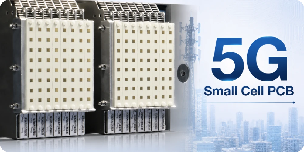
Table of Contents
- 5G Small Cell PCB Requirements Depend on the Radio Architecture
- FR1 and FR2 Small-Cell Boards: Different Manufacturing Priorities
- Low-Loss and Hybrid PCB Stackups for RF Plus Digital Processing
- RF Launches, Via Transitions, Reference Planes, and Copper Surface Effects
- HDI, BGA Assembly, Power Amplifier Thermal Paths, and Shielding
- Inspection and Test: What a PCB Manufacturer Can Verify Before System RF Qualification
- 5G Small Cell PCB RFQ Checklist for Fabrication and Turnkey PCBA
A 5G small cell PCB can mean very different hardware depending on whether the product is an integrated small cell, a radio unit within a disaggregated architecture, an indoor enterprise node, or another compact RAN implementation. Small Cell Forum reference material explicitly recognizes multiple 5G small-cell architectures and product types, so there is no universal “5G PCB stackup.” The manufacturing plan must follow the actual 3GPP NR frequency range, RF front-end architecture, baseband/PHY partition, power level, antenna implementation, enclosure, and cooling method. Highleap Electronics supports 5G communication PCB manufacturing, low-loss multilayer fabrication, HDI structures, and turnkey assembly for telecom hardware built to customer-approved RF and digital design data.
1. 5G Small Cell PCB Requirements Depend on the Radio Architecture
A 5G small cell may integrate baseband processing, radio functions, RF front end, timing, power conversion, network interfaces, and antennas in one enclosure. Other designs separate functions across radio and digital boards. Small Cell Forum’s 5G work also describes integrated and disaggregated product configurations, which is why a PCB supplier should ask what the board actually does before proposing materials or processes.
1.1 Radio Board and Digital Board May Have Different Optimal Constructions
A radio board prioritizes RF loss, phase consistency, isolation, thermal management, and connector/antenna transitions. A digital board may prioritize high-speed SerDes, DDR memory, processor escape routing, power integrity, and dense BGA assembly. Some products combine both on one mixed-material PCB; others use separate boards connected through high-speed interfaces.
1.2 Do Not Use “5G” as a Material Specification
The term 5G says nothing about the exact Dk, Df, copper profile, layer count, or via technology required. These depend on the operating bands, route lengths, modulation/error-vector-margin budget, connector architecture, and digital interfaces. A lower-loss laminate may be essential in one design and unnecessary in another.
1.3 Product Qualification Is Broader Than PCB Manufacturing
The finished small cell may need 3GPP radio conformance work, operator qualification, EMC, safety, environmental, and regional approvals. PCB fabrication and PCBA testing support repeatability but do not replace those system-level programs.
| Small-Cell Board Domain | Possible Construction Direction | Manufacturing Priority |
|---|---|---|
| FR1 radio / transceiver board | Multilayer FR-4 or lower-loss construction depending on loss budget. | Controlled impedance, RF launches, material consistency, shielding and thermal paths. |
| FR2 radio / antenna-related hardware | More geometry-sensitive RF structures; material and integration depend heavily on module/antenna architecture. | Tighter control of dielectric geometry, transitions, copper profile, surface treatment and mechanical registration. |
| Digital processing / baseband | High-layer-count or HDI construction around dense BGA/SoC and memory interfaces. | BGA escape, microvias, impedance, power integrity, warpage and X-ray inspection. |
| Power amplifier / power conversion | Heavy local copper, thermal vias, heat spreaders or other defined heat paths. | Copper geometry, via fill/cap, thermal interfaces and assembly sequence. |
| Hybrid RF + digital board | Low-loss material only where electrically justified, combined with other laminate systems when compatible. | Hybrid lamination compatibility, registration, controlled depth/vias and material traceability. |
2. FR1 and FR2 Small-Cell Boards: Different Manufacturing Priorities
3GPP NR specifications distinguish FR1 and FR2 operation; newer specifications further distinguish FR2-1 and FR2-2. For PCB manufacturing, the useful input is the actual operating band, RF architecture, critical interfaces, and channel requirements—not a generic “5G” or “FR2” label. A small-cell product can therefore require very different board constructions depending on the radio implementation.
2.1 FR1 Small Cells Often Mix RF and High-Speed Digital on Multilayer PCBs
FR1 designs can use conventional PCB transmission structures over practical distances, but loss, impedance, isolation, and power-amplifier thermal performance remain important. Low-loss hydrocarbon/ceramic or advanced high-speed laminate families may be used where the RF or digital channel budget requires them.
2.2 Is Every 5G Small Cell a mmWave PCB?
No. Many 5G small-cell products operate in FR1 and are not millimeter-wave boards. FR2 designs operate at millimeter-wave frequencies, where interconnect loss and transition sensitivity can become much more important. Some architectures minimize PCB RF path length by integrating antennas and front-end electronics in modules; where the main PCB still carries mmWave structures, material tolerance, copper roughness, registration, surface finish, and launch geometry require tighter control.
2.3 The Manufacturer Needs the Actual Band and Critical Nets
An RFQ that says only “5G board” is not enough. At minimum, identify which layers and interfaces are RF-critical, the relevant impedance structures, target materials, acceptable substitutions, and any coupon or test requirements. This lets the fabricator focus process control on the structures that drive performance.
3. Low-Loss and Hybrid PCB Stackups for RF Plus Digital Processing
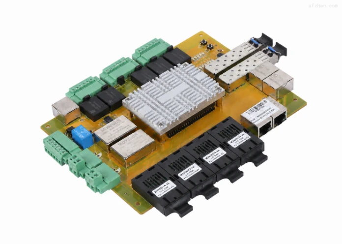
Small cell hardware frequently needs both RF performance and cost-effective multilayer routing. A hybrid stackup can place low-loss RF material only where it provides value while using FR-4-family or high-speed digital materials elsewhere, but mixed-material lamination must be engineered carefully.
3.1 Does Every 5G Small Cell PCB Need Rogers or PTFE?
No. A 5G small-cell PCB does not automatically require Rogers, PTFE, or any single laminate family. Material selection should follow the operating band, insertion-loss budget, RF path length, digital channel requirements, thermal/reliability needs, cost, and overall architecture. A hybrid RF / FR-4 stackup can be useful when low-loss material is justified only on selected layers, but mixed-material lamination must be reviewed for compatible dielectric thicknesses, cure behavior, dimensional stability, and bonding construction.
Highleap works with RF and lower-loss materials used in telecom products, including the types described in our RF PCB material selection resources. The final material callout and any approved equivalent criteria should remain tied to the customer’s electrical and reliability requirements.
3.2 Dk Is Not a Single Universal Number
Laminate datasheets may list different Dk values depending on test method and frequency. Designers should use the value appropriate to their field solver and material model, then correlate fabricated coupons or test structures as needed. The PCB factory should not substitute a laminate merely because two datasheets show a similar headline Dk.
3.3 Copper Profile Can Affect Loss
Lower-profile copper can reduce conductor loss on high-frequency paths, but the chosen copper foil also affects adhesion, fabrication behavior, and availability. If copper profile is electrically important, specify it in the stackup or material callout instead of assuming all copper foils are equivalent.
Highleap Electronics • PCB Manufacturing & PCBA
Review Your 5G Small Cell PCB Project
Send the RF stackup, radio architecture, thermal plan, BOM, mechanical constraints and test requirements for small-cell PCB and PCBA review.
4. RF Launches, Via Transitions, Reference Planes, and Copper Surface Effects
The weakest RF point is often a transition rather than a long straight trace. Connectors, vias, layer changes, component pads, filter launches, and transitions into RF modules introduce discontinuities.
4.1 Via Transitions Need Return-Path Design
A signal via should be considered together with nearby ground vias, antipad geometry, reference-plane changes, and unused stub length. Our RF PCB via design guide covers the manufacturing variables behind these transitions. Back-drilling or blind vias can reduce stub effects when the channel model shows that the improvement is necessary. For manufacturing, controlled-depth requirements must be stated clearly in the drill table.
4.2 Connector Launches Should Be Frozen With the Stackup
Coaxial or board-to-board RF connectors have recommended land patterns, but the optimum PCB launch also depends on dielectric thickness and reference geometry. Pad/antipad modifications during CAM can change return loss. Critical launches should be marked as do-not-modify areas unless engineering approves a change.
4.3 Surface Finish Is Part of the RF and Assembly Tradeoff
ENIG, immersion silver, OSP, and other finishes have different assembly, storage, planarity, contact, and RF implications. The best choice depends on the exposed RF structure, connector contact requirements, fine-pitch assembly, shelf life, and customer process. Highleap’s PCB surface finish guide can be used to discuss these tradeoffs before fabrication release.
5. HDI, BGA Assembly, Power Amplifier Thermal Paths, and Shielding
Small cells often combine dense processors, FPGAs/SoCs, RF transceivers, power amplifiers, clocking, memory, and power conversion in a constrained enclosure. Highleap supports high-frequency/RF and HDI PCB fabrication, component sourcing, BGA/SMT assembly, shielding integration, AOI/X-ray inspection and customer-defined functional or RF testing where a documented method and limits are supplied. The PCB has to support both routing density and heat removal.
5.1 HDI Can Keep High-Speed and RF Paths Short
Microvias, via-in-pad, buried vias, and sequential build-up structures allow dense BGA escape and reduce the need for long dog-bone routing. These features should be chosen based on package pitch and channel requirements. Highleap’s HDI PCB fabrication supports designs that require laser-drilled interconnects and compact routing.
5.2 Power Amplifiers Need a Defined Heat Path
RF power devices may use exposed thermal pads, copper coin structures, thermal via arrays, heat spreaders, or direct interfaces to a chassis. RF and microwave PCB thermal management must be defined together with the enclosure and mechanical cooling path. The most effective method depends on dissipated power, package, allowable temperature rise, and mechanical cooling design. Manufacturing should preserve the via fill/cap and copper structures required by the thermal model.
5.3 Shielding Changes Assembly Sequence
RF shielding frames, covers, absorbers, thermal pads, and mechanical heat spreaders can require a defined assembly order. Shield-frame paste volume, grounding pads, coplanarity, and rework access should be considered during DFA. Highleap’s BGA and SMT assembly process can incorporate these project-specific mechanical and soldering steps.
6. Inspection and Test: What a PCB Manufacturer Can Verify Before System RF Qualification
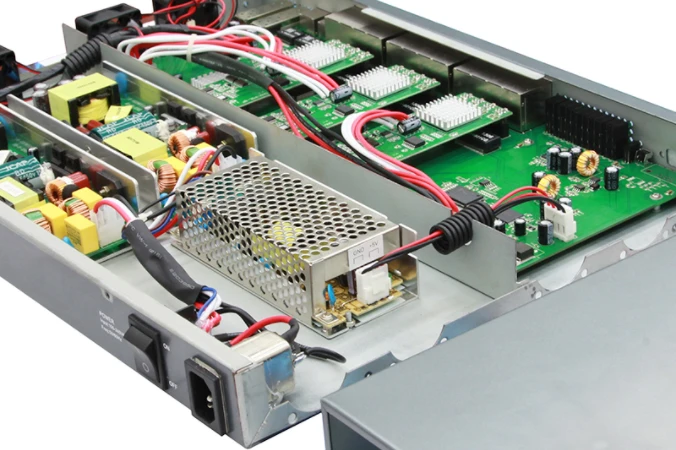
A manufacturing test plan should verify the attributes the factory can control and clearly separate them from radio-system qualification.
6.1 Bare-Board Controls
Relevant checks can include electrical continuity/isolation, dimensional inspection, controlled-impedance coupons, microsection analysis, plating verification, solder-mask/finish inspection, and material/lot documentation when required. RF test coupons may also be used if the customer provides the structure and measurement method.
6.2 Assembly Controls
SPI, AOI, and X-ray are selected according to package risk. X-ray is particularly useful for BGA/LGA/QFN and thermal-pad joints that cannot be seen directly. First-article inspection can verify component identity, orientation, placement, mechanical hardware, and shield assembly before the full lot proceeds.
6.3 Can a PCB Manufacturer Perform 5G Product Certification?
Routine fabrication and assembly inspection do not constitute 3GPP, operator, OTA or regulatory certification. A PCBA factory can perform power-up, programming, network communication, timing checks, digital I/O, and customer-defined conducted RF PCB testing when test access, calibrated equipment, software, fixtures and pass/fail limits are available. 3GPP conformance, operator acceptance, OTA antenna performance, and regulatory qualification remain separate system-level activities.
7. 5G Small Cell PCB RFQ Checklist for Fabrication and Turnkey PCBA
A technically complete small-cell RFQ should include:
- Gerber/ODB++ data, drill files, fabrication drawing, and panel constraints if any
- Full stackup with exact laminate, prepreg/core thickness, copper weight, and copper profile requirements where critical
- FR1/FR2 application context, actual operating bands, and identification of RF-critical layers/interfaces
- Controlled-impedance targets, tolerances, and coupon requirements
- Back-drill, blind/buried via, microvia, via-in-pad, and fill/cap requirements
- Surface-finish and exposed-RF-copper requirements
- BOM with RF components, processors, power devices, clocks, connectors, and approved alternates
- Pick-and-place and assembly drawings, shield/heatsink/thermal-interface details
- Programming, calibration, functional test, and RF test procedures
- Material traceability, inspection reports, and change-control requirements for production
For new radio hardware, a controlled prototype PCB and pilot PCBA build helps correlate material, stackup, RF launches, thermal design, and assembly with measured system performance before volume release. Highleap Electronics can review the manufacturing data and quote PCB fabrication, component sourcing, assembly, and project-defined inspection/testing scope. For related radio-board production considerations, see our RF PCB manufacturing for 5G devices resource.

Recommended Posts

TMM4 Filter PCB Manufacturing
TMM4 filter PCB manufacturing is controlled by the...

TMM3 PCB Manufacturing for RF Modules
TMM3 PCB manufacturing is most useful where the RF module...

TMM6 PCB Fabrication
TMM6 fabrication is the process-control page for a mid-Dk...

TMM10 PCB Manufacturing for Compact RF Designs
Table of contentsHow TMM10 Shrinks RF StructuresTMM10 vs...
How to get a quote for PCBs
Let’s run DFM/DFA analysis for you and get back to you with a report. You can upload your files securely through our website. We require the following information in order to give you a quote:
-
- Gerber, ODB++, or .pcb, spec.
- BOM list if you require assembly
- Quantity
- Turn time
For PCBA services, please provide your BOM (Bill of Materials) and any specific assembly instructions. We also offer DFM/DFA analysis to optimize your designs for manufacturability and assembly, ensuring a smooth production process.