
AD350A PCB Manufacturing for 5G and WiFi

For AD350A boards, the manufacturing review should connect the RF layers to the digital and power sections of the finished stackup. The page therefore emphasizes hybrid construction, impedance definition, registration, RF-critical geometry and quotation inputs instead of repeating a material-properties overview.
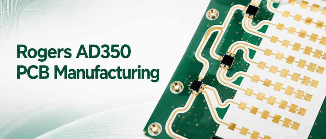
Figure 1. Rogers AD350A PCB manufacturing
AD350A PCB manufacturing for 5G and WiFi boards benefits from treating the RF layer and the production stackup as one controlled system. The design should identify which dielectric thicknesses and copper interfaces are carrying the RF budget before the board enters CAM. Rogers AD350A PCB manufacturing is used for commercial RF boards that need Dk 3.5 class performance, practical fabrication, and stable assembly yield. AD350A is commonly considered for sub-6 GHz RF hardware, Wi-Fi RF boards, antennas, filters, and cost-sensitive microwave assemblies. Highleap Electronics reviews laminate, copper, stackup, finish, connector areas, and PCBA needs before release.
Table of Contents
Material scope: This page concerns PCB fabrication using the specified Rogers material. Highleap Electronics manufactures the finished board and PCBA; laminate manufacturing and material sales are outside our service scope.
When AD350A Is the Right PCB Material
AD350A is used for commercial RF boards that need practical cost control, stable Dk 3.5 class performance, and reliable volume production. It is suitable for sub-6 GHz 5G hardware, Wi-Fi RF boards, antennas, filters, gateways, and industrial wireless products where the design must balance RF behavior with fabrication and assembly yield.
This material is usually a production decision as much as an RF decision. The stackup should support the impedance target without pushing trace width too tightly, the surface finish should support connector and shield soldering, and the selected process should be stable enough for repeat orders after prototype approval.
AD350A Is a Cost-and-Yield Decision for Commercial RF Boards
AD350A should not be treated like a maximum-performance microwave laminate. Its value is in commercial RF designs where the buyer needs stable RF behavior, manufacturable geometry, and production cost control. That means the quote review must include both RF and assembly details, especially when the product is a 5G sub-6 GHz, Wi-Fi, antenna, gateway, or industrial wireless board.
The main topic is cost-and-yield balance. Highleap checks whether the stackup can meet the impedance target without unnecessary line-width pressure, whether the selected finish supports connector soldering, whether RF shields or thermal pads affect assembly yield, and whether the design can move from prototype to repeat production without a material or process change. If a cheaper stackup creates tight trace widths, poor soldering access, or unstable supply, the apparent material saving can disappear during production.
An AD350A RFQ quote should separate must-have RF requirements from optional preferences. Frequency range, impedance tolerance, connector type, surface finish, solder mask clearance, assembly side, panel quantity, and annual demand all affect the most practical process choice. For commercial products, the best result is usually not the most exotic process; it is the process that reaches the RF requirement with stable yield.
- Use AD350A when the product needs commercial RF performance with manufacturable cost control.
- Review RF stackup and assembly access together so connector and shield areas do not create yield problems.
- Confirm prototype and production requirements at the same time to avoid later material or process changes.
AD350A RF Properties That Matter in Commercial PCB Production
| Item | Manufacturing meaning |
|---|---|
| Dk 3.5 class material | Supports compact RF layouts without the extreme feature sensitivity of very high-Dk laminates. |
| Commercial RF fit | Good candidate when cost, manufacturability, and RF stability must be balanced. |
| Copper and finish | Finished conductor geometry and solder finish affect loss, launch quality, and assembly yield. |
| Assembly planning | RF connectors, shields, thermal pads, and test points should be reviewed with fabrication. |
DFM and Stackup Review Before Quoting
A reliable quote starts with the complete Gerber set, drill files, netlist, board outline, stackup drawing, material callout, copper weight, surface finish, solder mask notes, impedance targets, and any assembly requirements. Highleap checks whether the design can be fabricated repeatably before tooling starts.
| DFM item | What to check |
|---|---|
| Panel yield | Balance RF geometry with practical trace/space, routing, and solder mask limits. |
| Connector areas | Check launch geometry, plating, finish, and mechanical reinforcement if needed. |
| Volume production | Lock stackup, panel format, inspection plan, packaging, and repeat-order controls. |
Manufacturing Process Controls
The process route should be selected before material is released to production. Typical controls include material verification, inner layer inspection, lamination review, drill quality, hole-wall preparation, copper plating, solder mask registration, surface finish, routing accuracy, electrical test, and final inspection. Highleap reviews the finished stackup, impedance structures, via transitions and copper geometry before fabrication. For production lots, the inspection plan can combine standard PCB checks with controlled-impedance verification where specified in the drawing. Exact material property values should be checked against the current supplier documentation for the specified grade and construction.
For recurring commercial builds, keep the approved stackup, copper construction, panelization, RF test method and PCBA process stable. Changes to connector areas, shields, thermal pads or solder-mask openings should be reviewed as production changes because they can alter both RF behavior and assembly yield.
RFQ Package and Production Records
AD350A is suitable for commercial antennas, sub-6 GHz 5G equipment, Wi-Fi 6/7 RF boards, industrial RF controls, filters, couplers, and communication modules that need stable production at practical cost.
Send Gerber files, drill data, stackup, AD350A thickness, copper weight, finish, impedance table, connector details, BOM and centroid if assembly is needed, prototype quantity, production quantity, and annual forecast.
For AD350A commercial builds, useful production evidence includes impedance coupons or reports where specified, first-article inspection, electrical test results, surface-finish records and PCBA inspection records. The report set should match the released drawing instead of adding generic certificates that do not affect acceptance. For quotation, send the RF band, layer construction, board size, copper, impedance targets, quantity and assembly scope. These inputs allow the quote to distinguish a simple RF board from one that needs tighter process control or additional testing.

Recommended Posts

TMM4 Filter PCB Manufacturing
TMM4 filter PCB manufacturing is controlled by the...

TMM3 PCB Manufacturing for RF Modules
TMM3 PCB manufacturing is most useful where the RF module...

TMM6 PCB Fabrication
TMM6 fabrication is the process-control page for a mid-Dk...

TMM10 PCB Manufacturing for Compact RF Designs
Table of contentsHow TMM10 Shrinks RF StructuresTMM10 vs...
How to get a quote for PCBs
Let’s run DFM/DFA analysis for you and get back to you with a report. You can upload your files securely through our website. We require the following information in order to give you a quote:
-
- Gerber, ODB++, or .pcb, spec.
- BOM list if you require assembly
- Quantity
- Turn time
For PCBA services, please provide your BOM (Bill of Materials) and any specific assembly instructions. We also offer DFM/DFA analysis to optimize your designs for manufacturability and assembly, ensuring a smooth production process.