
AlN Ceramic PCB Manufacturer for High-Thermal-Performance Electronics
Highleap Electronics supplies custom AlN ceramic PCB manufacturing for designs that need an electrically insulating substrate and a high-conductivity thermal path. We support aluminum nitride ceramic circuit requirements for laser-diode assemblies, high-power LEDs, RF power electronics, SiC/GaN modules and precision electronic packages, with agreed metallization, fabrication and assembly scope.
AlN is aluminum nitride (the final character is a lowercase “l”); it is not alumina (Al2O3). Board geometry, substrate grade, copper pattern, bonding method and the final heat-sink interface determine whether an AlN substrate is right for a particular product.
Custom AlN Ceramic PCB Manufacturer

Highleap manufactures and sources aluminum nitride ceramic circuit boards as a distinct substrate family within its ceramic PCB offering. The project begins with a qualified substrate grade and a metallization pattern, not an FR-4 stack-up. Highleap’s ceramic circuit board fabrication portfolio describes AlN, alumina and silicon-nitride choices alongside metallization and follow-on assembly.
AlN is selected when the design needs electrical insulation with much higher bulk thermal conductivity than typical alumina. A Kyocera AlN substrate family, for example, specifies thermal conductivity of 150 W/(m·K) or higher; actual values depend on the grade, test method and operating temperature. Substrate conductivity is only one input to junction-to-case temperature: die attach, copper coverage, ceramic thickness, solder voids and heatsink contact can dominate the completed module.
High-thermal-conductivity electrically insulating ceramic for compact heat sources. Published material grades vary significantly; confirm the actual vendor grade and temperature basis.
Often lower-cost ceramic for thick-film circuits and many power or sensor boards when the full heat path meets the thermal budget.
When should an OEM choose AlN instead of alumina ceramic?
When the measured or modeled thermal resistance through the substrate is a limiting part of the die-to-heatsink path, not simply because an AlN datasheet reports a larger conductivity number. Supplier AlN grades may publish values around 150–240 W/m·K, while specific alumina grades are often near 20–30 W/m·K at room temperature. These are material-grade examples, not a promised finished-board performance rating. Die attach, patterned metal, thickness and heatsink interface must be evaluated as well.
Is AlN a PCB material or a ceramic power substrate?
Both terms appear in procurement documents. In practice, the specification must say whether the product is a patterned metallized ceramic board, a DBC/AMB power substrate, a thin-film circuit or a packaged module. Their copper thicknesses, feature sizes and assembly processes are not interchangeable.
AlN Ceramic Substrates for Laser Diodes and High-Power LEDs

AlN ceramic LED boards and laser-diode substrates use the ceramic body as part of the thermal path while preserving electrical isolation. Typical buy-to-print products include high-power LED array substrates, UV and IR emitter carriers, laser-diode submounts, optical sensor packages and compact illumination modules. Highleap can assess these projects through its custom ceramic substrate manufacturing resources with dimensions and attachment requirements defined by the OEM.
For a laser-diode submount, a drawing should identify die location, attach metallization, metal thickness, flatness, heat spreading footprint and any wire-bond pads. For an LED array, include LED manufacturer part numbers, package orientation, thermal pad structure, solderable finish, mounting pattern and the intended carrier or heatsink. If the customer needs thermal resistance or optical testing, the relevant fixture and test limits must be agreed separately.
Can an aluminum nitride LED circuit board replace an aluminum-core PCB?
Not as a drop-in substitution. Aluminum-core boards contain a separate electrically insulating dielectric between their circuit copper and metal core. AlN ceramic is itself insulating, with a different CTE, fracture behavior, metal attachment scheme and fastening design. The OEM must verify thermal, electrical and mechanical consequences. Highleap also offers metal-core LED PCB alternatives when those better match the design.
AlN DBC and AMB Substrates for SiC/GaN Power Modules
AlN DBC and AlN AMB substrates address power modules that need copper conductors bonded to electrically insulating ceramic. These are distinct copper-to-ceramic technologies. Highleap publishes direct-bonded-copper substrate manufacturing and active-metal-brazed ceramic substrate options as relevant product lines; the selected route must be compatible with the exact AlN grade and mechanical/reliability specification.
| Feature | What the buyer must define | Why it affects an AlN module |
|---|---|---|
| Ceramic material and thickness | Approved AlN grade, nominal thickness, finish, flatness. | Thermal path, stiffness, fracture risk and module height. |
| Copper metallization | Pattern, copper thickness, copper-to-ceramic bond system. | Current flow, heat spreading and thermal cycling of the interface. |
| Clearances and isolation | High-voltage spacing, dielectric test and intended potting if applicable. | Electrical safety cannot be inferred from material name alone. |
| Module attachment | Solder/sintered attach, baseplate, clamping, thermal compound. | Contact resistance and mismatch stresses can dominate field behavior. |
A copper-bonded AlN substrate with large traces is not automatically equivalent to a fine-feature AlN microelectronic circuit. AMB may be preferred for certain high-reliability power structures; DBC may be a practical alternative depending on design and process qualification. Highleap should quote the approved process and required bond test records rather than representing all ceramic metallization systems as equivalent.
Bonded copper foil for designated power substrate geometry; insulation, copper thickness and pattern gaps are joint design constraints.
Active-metal-brazed metal-to-ceramic attachment selected to meet a specific power-cycle and interface requirement; reliability must be qualified.
Deposited/seeded and plated copper patterns suited to different feature-size and thickness combinations from thick bonded foil.
Is AMB automatically more reliable than DBC for every power module?
No. The qualified module design—including ceramic thickness, copper pattern shape, substrate material, attach layer, cycling profile and acceptance testing—sets the result. Choosing AMB by name cannot guarantee thermal-cycle lifetime. Send the temperature range, cycle profile and module interface specification with the RFQ.
Does AlN DBC guarantee the thermal cycling life of a SiC module?
No. Ceramic composition, copper pattern, corner geometry, sintered or soldered interfaces, wire bonds, housing and the actual mission profile all affect reliability. Ask for the cycle conditions, sample size, acceptance criteria and test owner rather than a generic lifetime number.
AlN DPC and Thin-Film Ceramic PCB Manufacturing

AlN DPC and thin-film ceramic circuits serve finer conductors or smaller pads than many heavy-copper power substrates. Highleap’s thin-film metallized ceramic PCB offering is relevant where photonics, RF or microelectronic assemblies require fine geometry or bond-compatible surface properties. Ask which sputtering, deposition, imaging, plating and final-finish route is actually available for the requested AlN grade.
An AlN DPC project may require a plated via structure, patterned conductor layers and defined surface finish. A thin-film circuit may instead be selected for small line widths or precision metal stacks. The two labels do not describe identical thicknesses or process windows. Manufacturing acceptance should use a defined mask/line map, conductor thickness, via termination, isolation test and pad adhesion method.
Can a custom AlN ceramic PCB have multiple layers or metallized vias?
Two-sided patterned metallization and selected via approaches are different from a genuine multilayer co-fired ceramic package. Co-fired multilayer AlN constructions exist in specialist ceramic packaging, but they are not automatically included in an AlN DBC/DPC order, and conventional LTCC processes should not be described as an ordinary AlN upgrade. Identify the number of independent conductor layers, via function, fired or finished dimensions and specialist process route for a separate feasibility review.
Can AlN ceramic PCB have metallized vias or two-sided circuits?
Certain ceramic metallization routes can support vias and more than one patterned side, but the available via aspect ratio, hole finish and process sequence are not the same as FR-4 plated-through-hole PCB fabrication. Provide the cross-section and request a project-specific route review.
AlN Ceramic Boards for RF Power Amplifiers and Microwave Devices
AlN ceramic PCBs are useful where thermal density, insulation and circuit packaging have to work together. Highleap can assess AlN substrates for RF amplifier stages, GaN power devices, SiC switching modules, compact DC/DC power stages and precision thermal packages. Each is a different assembly specification: an RF amplifier prioritizes controlled RF geometry and ground continuity, while a switching power module may prioritize thick copper, dielectric isolation and thermal-cycle behavior.
Where the product includes a separate standard multilayer controller, Highleap can coordinate a ceramic power substrate with a conventional controller PCB manufacturing package. It is important not to conflate ceramic substrate qualification with system-level EMC, RF characterization, functional-safety certification or inverter testing. The power-electronics PCB manufacturing service provides adjacent options for the control-board portion.
How should AlN PCB requirements differ for RF and high-voltage power?
RF buyers should prioritize the applicable metallization, conductor geometry, ground connection, frequencies and assembled device performance. Power-module buyers should specify copper thickness, isolation, operating temperature, thermal-cycle profile and attach/mounting interfaces. Both still need the approved AlN grade and mechanical drawing.
Aluminum Nitride Ceramic PCB Assembly and Die Attach

Highleap can coordinate assembly of compatible AlN ceramic circuits in addition to bare ceramic fabrication. Possible project-defined operations include SMT component placement, die attach, wire bonding, soldering or sintered attachment, inspection and module-level testing. The actual attach technology and specialist production site should be confirmed with the customer’s process and packaging requirements, not assumed from conventional SMT capability.
Unlike a conventional FR-4 board, an AlN substrate may be thin, brittle and sensitive to point loading. The fixture, vacuum pick-up, clamping and oven profile need to match the ceramic geometry. Metal bond pads, flux residues and cleaning restrictions must suit the selected device and surface finish. A power assembly with mounted MOSFETs may require void limits under the die; a laser module may require positional alignment and bond strength evidence.
Can Highleap supply a complete die-attached AlN power module?
Highleap can quote ceramic substrate fabrication and discuss a coordinated assembly package. Die attachment, sintered interfaces, wire bonding, encapsulation and completed-module electrical or thermal qualification are specialized operations; they must be listed individually with the responsible process route and acceptance records, rather than assumed from standard SMT assembly.
Highleap’s PCB assembly and component integration services can be considered for the surrounding electronics, with a separate process definition for any chip-level operations. Where microelectronic bonding is specified, get the bonding method and fixture ownership written into the assembly scope.
Is a completed AlN ceramic module included with a bare PCB quotation?
No. A bare metallized substrate and a populated ceramic assembly have different BOMs, tooling, handling, tests and liabilities. Request separate deliverables for ceramic fabrication, components, attach operations, module inspection and any finished-device validation.
AlN Ceramic Substrate Inspection and Thermal Specifications

The acceptance plan for AlN ceramic PCB manufacturing must verify the defined drawing, electrical insulation and metallization quality. Highleap can discuss incoming substrate identification, dimensional/flatness inspection, conductor pattern checks, continuity and isolation, finish thickness and project-specific bond or reliability records. The exact inspection method and delivery documentation should be agreed with the nominated ceramic production route.
| Acceptance subject | Typical requested evidence | Important boundary |
|---|---|---|
| AlN substrate | Grade and thickness identity, chip/crack inspection, flatness. | Nominal data-sheet conductivity is not a measured module thermal resistance. |
| Metallization | Circuit dimensions, metal thickness, adhesion/bond evidence as required. | A metal pattern passing electrical continuity may still fail the bond criterion. |
| Electrical isolation | Specified insulation/hipot test at stated voltage and duration. | System-level safety approval belongs to the finished product. |
| Assembled module | Die attach, bond inspection, functional/thermal tests as contracted. | AOI is not a substitute for optical or RF performance testing. |
Highleap’s PCB quality and inspection information helps explain the distinction between fabrication checks and assembled-product tests. A claimed 100% inspection needs its exact scope: which parameter, with what method and which acceptance limit. Test coupons or sample quantities must be identified for destructive adhesion or thermal-cycle qualification.
Approved material grade, thickness, dimensions, flatness and supplier property data.
Copper/metal dimensions, adhesion or bonding requirements, final finish and visual inspection.
Defined die or SMT attachment, void criteria, insulation/continuity checks and project-specific tests.
Can a supplier certify the thermal conductivity of each finished AlN PCB?
Thermal conductivity is generally a substrate-grade property with a material test method and supplier certificate. The completed board’s heat flow depends on patterned metal, attach layers and interfaces. If a production thermal measurement is required, specify the actual assembly and test fixture rather than assuming it is included in standard substrate inspection.
AlN Ceramic PCB Quotes and Custom Fabrication Requirements
Highleap quotes custom aluminum nitride ceramic boards from the released substrate and metallization specification. Lead time and price depend on the AlN grade, part size, thickness, pattern definition, DBC/DPC/thin-film route, substrate utilization, hole/cavity needs, finish, inspection level and quantity. A power module and a laser-diode submount of similar dimensions can have entirely different processing costs.
- Material and mechanics: AlN grade, manufacturer restriction if any, nominal thickness, outline, tolerances, surface condition and flatness.
- Conductor definition: Gerber/DXF, metallization process, thickness, finish, circuit side, pad locations, vias and isolation spaces.
- Assembly scope: bare substrate or populated unit; die/LED BOM, bond pad scheme, attach and thermal-interface instructions.
- Acceptance: inspections, dielectric test, bond/void requirements, reliability samples, packing and traceability.
- Commercial scope: prototype quantity, yearly forecast, release schedule and destination.
For detailed process restrictions on ceramics, Highleap’s ceramic board fabrication service information is a related resource. Send the full manufacturing package so the quote identifies each ceramic and assembly operation and excludes unrequested qualification work.
What drives the price of an AlN ceramic PCB?
The substrate material cost is only one factor. Yield, precision of the copper pattern, specialty finishes, plating/metal adhesion, thin-ceramic handling, destructive tests, die-attach tooling and low-volume setups may all influence the quotation. Requested quantities and exact drawing data are necessary for a defensible price.

Recommended Posts

Al2O3 Ceramic PCB Manufacturer for Precision Ceramic Circuits
HIGHLEAP ELECTRONICS · Aluminum Oxide Ceramic Circuit...
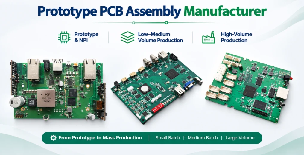
Prototype PCB Assembly Manufacturer
Highleap Electronics is a prototype PCB assembly...
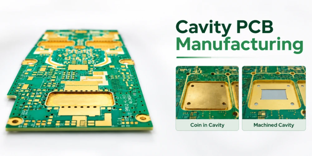
Special-Feature Circuit Boards for OEM Products
Highleap Electronics / PCB + PCBA...
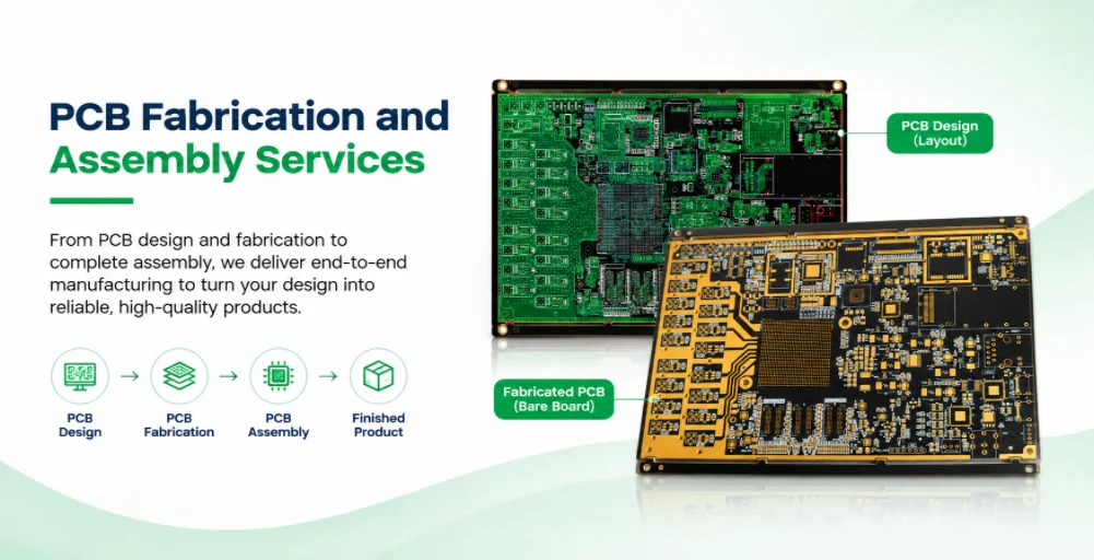
PCB Fabrication and Assembly Services
Highleap Electronics provides PCB fabrication and assembly...
How to get a quote for PCBs
Let‘s run DFM/DFA analysis for you and get back to you with a report. You can upload your files securely through our website. We require the following information in order to give you a quote:
-
- Gerber, ODB++, or .pcb, spec.
- BOM list if you require assembly
- Quantity
- Turn time
In addition to PCB manufacturing, we offer a comprehensive range of electronic services, including PCB design, PCBA, and turnkey solutions. Whether you need help with prototyping, design verification, component sourcing, or mass production, we provide end-to-end support to ensure your project’s success.
For PCBA services, please provide your BOM (Bill of Materials) and any specific assembly instructions. We also offer DFM/DFA analysis to optimize your designs for manufacturability and assembly, ensuring a smooth production process.