
Microstrips in High-Frequency PCB Design: Complete Guide

Introduction
High-frequency PCB design demands precise control over signal transmission to maintain integrity and minimize losses. Among the various transmission line structures available, microstrips in high-frequency PCB design stand out as the most widely adopted solution for RF and microwave applications. This surface-mounted transmission line configuration offers an optimal balance between performance, accessibility, and manufacturing cost-effectiveness. As operating frequencies continue to rise in modern electronics, understanding microstrip characteristics becomes essential for engineers developing wireless systems, radar applications, and high-speed digital interfaces.

Microstrip
What Is a Microstrip in PCB Design?
A microstrip consists of a conductive signal trace positioned on the outer layer of a PCB, separated from a ground plane by a dielectric substrate. This seemingly simple structure creates a controlled electromagnetic environment where signal propagation occurs partially through the dielectric material and partially through the air above the trace. The dual-medium propagation path defines the microstrip’s unique electrical characteristics and determines its effectiveness in high-frequency applications.
The exposed nature of microstrips makes them particularly attractive for RF circuits requiring component mounting or probe access. This accessibility advantage, combined with straightforward manufacturing requirements, explains why microstrips remain the preferred choice for antenna feeds, RF interconnects, and impedance-matched transmission lines operating from MHz to GHz frequencies.
Microstrip vs Stripline: Key Differences in High-Frequency PCB Design
Understanding when to choose microstrips over striplines requires examining their fundamental structural and electrical differences. Each configuration offers distinct advantages that align with specific design requirements and constraints.
| Parameter | Microstrip | Stripline |
|---|---|---|
| Structure | Signal trace on outer layer above a ground plane | Signal trace sandwiched between two ground planes |
| Field Distribution | Partially in air and partially in dielectric | Entirely within the dielectric |
| EMI Susceptibility | Higher (open field, more radiation) | Lower (fully shielded) |
| Dielectric Constant (Effective) | Lower effective Dk due to air interface | Higher effective Dk, more consistent |
| Losses | Slightly higher due to radiation | Lower radiation loss but higher dielectric loss |
| Manufacturing Complexity | More complex (inner layer routing) | |
| Tuning and Access | Easier to probe and modify | Harder to access for testing |
| Typical Applications | RF feed lines, antenna connections, high-speed traces | Controlled impedance internal routing, sensitive analog signals |
In high-frequency PCB design, microstrips excel when surface accessibility and low-cost routing take priority, particularly in RF front-ends or antenna traces. Striplines provide superior shielding and consistent impedance control, making them suitable for dense multilayer boards or high-speed differential pairs. The selection between microstrip vs stripline configurations depends on operating frequency, signal sensitivity requirements, and available board stack-up options.

Microstrip vs Stripline
Key Design Parameters Affecting Microstrip Performance
Geometric Dimensions
The impedance and propagation characteristics of microstrips depend primarily on three geometric parameters: trace width (w), dielectric height (h), and copper thickness (t). The width-to-height ratio (w/h) serves as the primary determinant of characteristic impedance, with typical values ranging from 0.5 to 2.0 for standard 50-ohm designs. Copper thickness influences both the effective width and conductor losses, becoming increasingly significant at frequencies where skin depth approaches the conductor thickness.
Material Properties
Dielectric constant (Dk) directly impacts both the effective permittivity and signal velocity in microstrip structures. Lower Dk materials reduce the effective dielectric constant, improving signal speed and reducing dispersion at higher frequencies. Surface roughness at the conductor-dielectric interface introduces additional losses through increased effective resistance, particularly noticeable above 10 GHz where skin depth becomes comparable to roughness dimensions.
Environmental Factors
Solder mask overlays modify the effective dielectric constant of microstrips, typically increasing it by 0.2 to 0.5 depending on mask thickness and composition. Temperature variations cause dimensional and material property changes that shift impedance values, requiring careful consideration in designs operating across wide temperature ranges. Humidity absorption in certain dielectric materials can significantly alter Dk values, making material selection critical for environmentally exposed applications.
Signal Integrity and Loss Mechanisms in Microstrip Design
Conductor Losses
Skin effect forces high-frequency currents to concentrate near conductor surfaces, effectively reducing the cross-sectional area available for current flow. This phenomenon increases resistance proportionally to the square root of frequency, making conductor losses dominant at lower microwave frequencies. Surface roughness exacerbates conductor losses by increasing the effective path length and creating current crowding at surface irregularities.
Dielectric Losses
Dielectric loss tangent determines the energy dissipated as electromagnetic waves propagate through the substrate material. These losses increase linearly with frequency and become the dominant loss mechanism at millimeter-wave frequencies. High-frequency microstrip designs require low-loss materials with loss tangents below 0.002 to maintain acceptable insertion loss performance.
Radiation and Coupling
The partially open field structure of microstrips inherently radiates electromagnetic energy, particularly at discontinuities like bends, vias, and impedance transitions. This radiation contributes to insertion loss while potentially causing electromagnetic interference with adjacent circuits. Proper spacing between parallel microstrip traces minimizes crosstalk, with separation distances of at least three times the substrate height typically providing adequate isolation.
Impedance Control and Design Techniques
Impedance Calculation Methods
Accurate impedance prediction for microstrips requires sophisticated electromagnetic modeling tools or empirical equations that account for fringing fields and dispersion effects. Industry-standard calculators like Polar Si9000 and Keysight ADS provide reliable impedance predictions when supplied with accurate material properties and geometric dimensions. These tools incorporate corrections for solder mask effects, copper roughness, and frequency-dependent material properties essential for high-frequency microstrip optimization.
Return Path Management
Maintaining continuous return current paths beneath microstrip traces ensures predictable impedance and minimizes radiation. Splits or gaps in the reference plane force return currents to find alternate paths, creating impedance discontinuities and increased electromagnetic emissions. Strategic via placement and careful layer stack planning preserve return path integrity, particularly critical when microstrips transition between layers or cross power plane boundaries.
Geometric Optimization
Corner mitigation techniques, including chamfering or curving, reduce impedance discontinuities and minimize radiation at direction changes in microstrip routing. Maintaining constant trace width except at controlled impedance transitions prevents unwanted reflections that degrade signal integrity. Tapered transitions provide smooth impedance matching when connecting microstrips to components with different impedance requirements.

High Frequency Circuit Board Manufacturing
Materials and Manufacturing Considerations
High-Frequency Substrate Selection
Premium materials like Rogers 4350B, Taconic RF-35, and PTFE-based laminates offer the low loss tangent and stable dielectric constant essential for high-frequency microstrip applications. These materials maintain consistent electrical properties across temperature and frequency ranges, ensuring predictable performance in demanding environments. Material selection balances electrical performance requirements against cost constraints and manufacturing compatibility.
Surface Finish Impact
The choice between ENIG, immersion silver, and other surface finishes significantly affects high-frequency microstrip performance through variations in conductivity and surface roughness. Immersion silver provides excellent conductivity with minimal thickness variation, making it ideal for frequencies above 10 GHz. ENIG offers superior shelf life and solderability but introduces nickel’s magnetic losses that become significant at higher frequencies.
Manufacturing Tolerances
Controlling dielectric thickness variations to within ±10% ensures impedance tolerance remains within acceptable limits for most high-frequency applications. Copper weight consistency and etch factor control determine trace width accuracy, directly impacting impedance precision. Advanced manufacturing processes at facilities like Highleap Electronics achieve the tight tolerances necessary for reliable microstrip performance in demanding applications.
Common Mistakes in Microstrip Design
Impedance Discontinuities
Neglecting impedance control at layer transitions or component interfaces creates reflections that degrade signal quality and increase return loss. Failing to account for solder mask effects leads to impedance values shifting 5-10% from design targets. Inconsistent trace width due to poor etch compensation or design rule violations introduces distributed impedance variations that accumulate into significant performance degradation.
Reference Plane Violations
Routing microstrips across split planes or power plane boundaries disrupts return current flow, creating impedance discontinuities and electromagnetic radiation. Insufficient ground via density near layer transitions forces return currents through longer paths, increasing inductance and degrading high-frequency performance. Inadequate ground plane extension beyond trace edges reduces shielding effectiveness and increases unwanted coupling.
Material Property Assumptions
Using nominal dielectric constant values without considering lot-to-lot variations or frequency dependence leads to impedance mismatches in manufactured boards. Ignoring moisture absorption effects in hygroscopic materials causes performance drift in humid environments. Failing to account for temperature-dependent material properties results in impedance shifts that compromise system performance across operating temperature ranges.
Conclusion
Microstrips play a vital role in high-frequency PCB design, offering a balance of electrical performance, manufacturability, and cost efficiency. Their open-field structure makes them ideal for RF front-ends, antenna feed lines, and other high-speed signal paths where controlled impedance and minimal loss are crucial. By mastering the relationships between geometry, dielectric properties, and signal behavior, engineers can design microstrips that deliver stable performance even at GHz-level frequencies.
Achieving consistent results, however, depends not only on design precision but also on manufacturing expertise. Highleap Electronics provides:
- Precision impedance control through advanced fabrication and testing equipment
- High-frequency material expertise including Rogers, Taconic, and PTFE-based substrates
- Tight process tolerances ensuring consistent dielectric thickness and copper uniformity
- Comprehensive engineering support from impedance modeling to prototype validation
For engineers developing next-generation RF or high-speed digital systems, Highleap Electronics offers the manufacturing reliability and technical insight required for superior microstrip performance. Contact our engineering team today to discuss your high-frequency PCB design needs and explore how precision-controlled fabrication can enhance your product’s signal integrity and consistency.

Recommended Posts
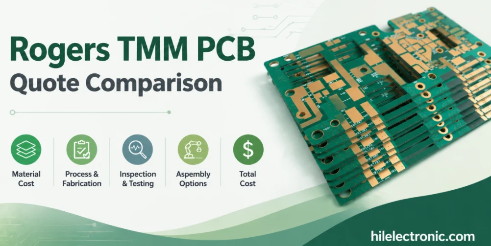
Rogers TMM PCB Quote Comparison and Cost Factors
Table of contentsCan Rogers TMM PCB Price Be Calculated...
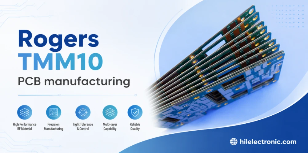
Rogers TMM10 PCB Manufacturing for RF Designs
Table of contentsHow TMM10 Shrinks RF StructuresTMM10 vs...
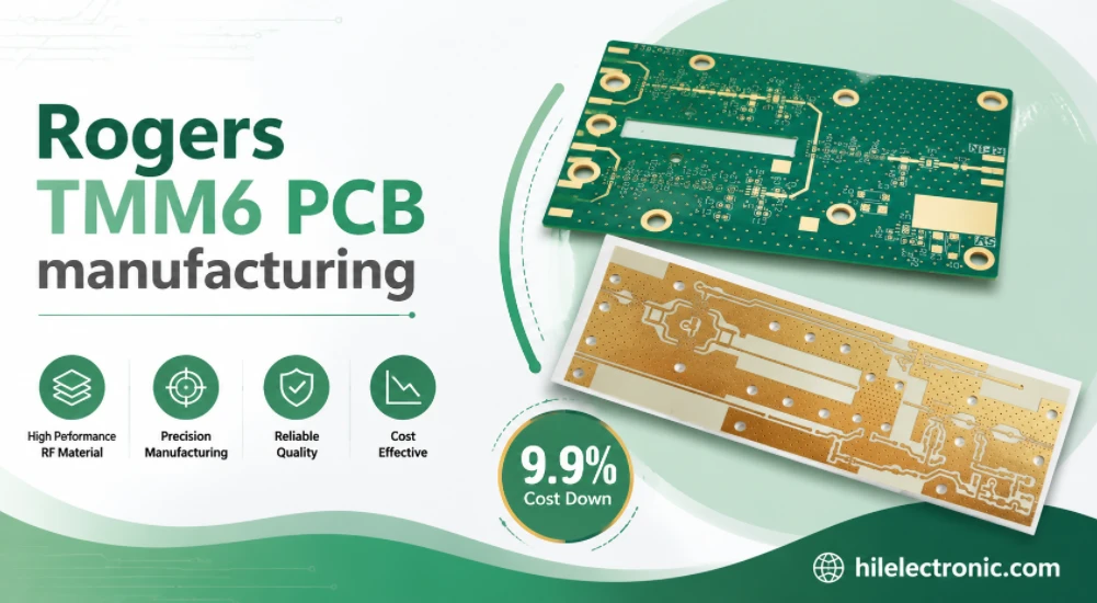
Rogers TMM6 PCB Manufacturing for Microwave Filters
Table of contentsWhy Microwave Filter Designers Use...

Taconic fastRise 27 Prepreg PCB Bonding and HDI Fabrication Service
Table of contentsWhat fastRise 27 Is—and What You Are...
How to get a quote for PCBs
Let‘s run DFM/DFA analysis for you and get back to you with a report. You can upload your files securely through our website. We require the following information in order to give you a quote:
-
- Gerber, ODB++, or .pcb, spec.
- BOM list if you require assembly
- Quantity
- Turn time
In addition to PCB manufacturing, we offer a comprehensive range of electronic services, including PCB design, PCBA, and turnkey solutions. Whether you need help with prototyping, design verification, component sourcing, or mass production, we provide end-to-end support to ensure your project’s success.
For PCBA services, please provide your BOM (Bill of Materials) and any specific assembly instructions. We also offer DFM/DFA analysis to optimize your designs for manufacturability and assembly, ensuring a smooth production process.