
TC350 PCB Manufacturing for RF Power Boards

TC350 PCB manufacturing for RF power boards should include the thermal path in the electrical release. High-power RF structures can meet the signal requirement and still fail at the assembly stage if copper, heat spreading and component interfaces were not planned together. Rogers TC350 PCB manufacturing is usually requested for one reason: the board must handle RF power and thermal load better than a standard FR4 stackup can. The buyer is not looking for a generic laminate overview. The buyer wants to know whether the supplier can keep RF loss, line control, heat spreading, and connector quality stable from first build to repeat order. For a power board using different dielectric families, mixed RF and FR-4 stackup engineering must establish a compatible bonding system and finished layer spacing.
Highleap Electronics treats TC350 builds as power RF boards first and laminate selections second. We review the transmission-line geometry, output network layout, copper spreading strategy, via-based heat path, grounding scheme, and connector or heat-sink interfaces before confirming the fabrication route. Related services include Rogers PCB manufacturing and high-frequency PCB fabrication.
TC350 production is treated around RF power-amplifier board construction. The review connects the RF path, thermal copper, board thickness, plated structures and assembly requirements so the finished PCB can be evaluated as a complete power/RF interconnect.
Where TC350 Fits in RF Power Board Manufacturing
TC350 is usually chosen for boards that must move RF power, not just RF signals
TC350 is commonly used in RF power amplifier boards, microwave transmit modules, RF feed structures, and communication hardware where dielectric stability and thermal behavior must be balanced together. The board is often expected to carry meaningful RF power while still maintaining controlled line geometry and consistent connector transitions.
That makes the sourcing discussion different from a low-power RF board. The manufacturing review has to consider not only electrical loss, but also how the layout moves heat away from active devices and whether the finished board can support stable assembly around the RF section.
Application context changes the right stackup
A TC350 board for an amplifier pallet is not reviewed the same way as a smaller signal-conditioning RF module. The first may prioritize copper spreading and thermal attachment. The second may care more about line repeatability, shielding, and connector density. Highleap therefore asks where the board sits in the final product before confirming a fabrication route.
How TC350 Affects RF Layout and Transmission Lines
The dielectric choice should be tied directly to the line model
TC350 only helps when the transmission-line design is documented clearly enough for fabrication. Highleap checks dielectric thickness, copper weight, reference plane continuity, connector launch geometry, and any RF transition that changes impedance along the route.
- 50 ohm line geometry and tolerance window
- Finished copper versus base copper assumption
- Reference plane integrity around the RF path
- Launch geometry at connectors, test ports, or module interfaces
Customers sometimes release the board files without the electrical assumptions behind them. That slows down the quote and increases the risk of building to the wrong copper or dielectric interpretation. When possible, we align the review with PCB impedance control targets before CAM release.
Signal performance and manufacturability should be reviewed together
On RF power boards, design choices that improve one parameter can make another harder to control. A narrow line may help the electrical model but become more sensitive to copper tolerance. A dense launch may reduce path length but complicate grounding and assembly. The practical answer is to review RF intent and manufacturing tolerance as one decision.
Heat Spreading, Copper Design, and Thermal Via Planning
Thermal design is usually the make-or-break part of the build
TC350 projects often include power devices, heat spreaders, or grounded metalwork that turn the PCB into part of the thermal path. If those details are not reviewed before fabrication, the board may pass bare-board inspection but still underperform in the amplifier assembly.
| Area | Typical risk | Review focus |
|---|---|---|
| Device pads | Poor heat transfer or solder voiding | Pad shape, copper balance, assembly method |
| Thermal vias | Incomplete heat path or solder loss | Via fill strategy, spacing, connection to planes |
| Heat-sink interface | Flatness and mounting inconsistency | Mechanical tolerance, finish, planarity |
For RF power boards, copper spreading is not just a thermal feature. It also affects return current flow and sometimes the RF grounding environment. That is why we review thermal patterns together with RF layout rather than after the stackup is frozen.
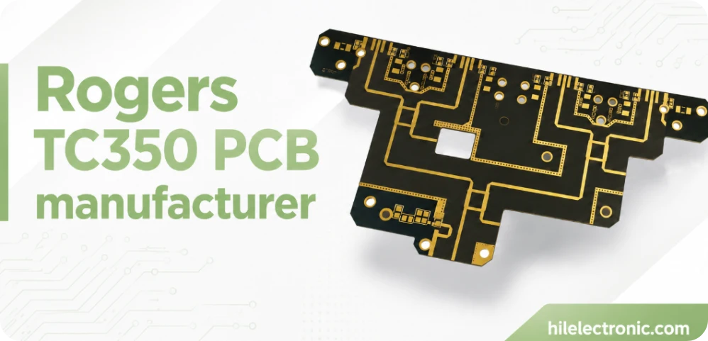
Material scope: This page concerns PCB fabrication using the specified Rogers material. Highleap Electronics manufactures the finished board and PCBA; laminate manufacturing and material sales are outside our service scope.
PTFE Processing Risks That Need Manufacturing Control
TC350 builds should not be treated like routine FR4 drilling and routing
PTFE-based and RF-oriented materials demand tighter control over drilling, routing, hole quality, and dimensional stability than ordinary multilayer FR4. If the fabrication team treats the board as a standard mechanical process, the electrical performance can drift before the assembly even starts. Highleap reviews the RF layers, copper distribution, plated structures and assembly pads around the power section. The manufacturing plan should make thermal interfaces and any heavy-copper or heat-transfer requirements explicit before fabrication and soldering. Exact material property values should be checked against the current supplier documentation for the specified grade and construction. Where the material shortlist includes TC600, TC600 fabrication for RF heat-flow requirements should be checked against the same electrical and mechanical acceptance criteria.
Highleap reviews hole quality, wall condition, edge definition, and panel handling before releasing a TC350 build. If the design mixes RF layers with denser mechanical features, we also evaluate how that balance affects yield and repeatability.
Panel strategy influences final consistency
Small RF boards often look simple but become harder to control when the panel is poorly planned. Break-off features, edge clearance, copper balance, and fixture requirements can all influence dimensional stability, especially when the build also includes a heat sink, connector cluster, or grounded shield frame.
Connector Launches, Shielding, and Assembly Review
The board is only one part of the RF path
Even a well-fabricated TC350 board can lose performance if the connector transition, shield attachment, or metal contact scheme is weak. Highleap reviews launch geometry, soldered connector pads, mounting hardware, and any local reinforcement needed around the RF interface.
Assembly readiness is also part of the quote. If the board needs soldered connectors, hand-placed components, test fixtures, or specific cleaning controls, that should be included up front so the RFQ reflects the real build scope. For projects moving beyond bare boards, we align that review with RF PCB manufacturing requirements.
Inspection should match the board’s failure modes
RF power boards do not all need the same inspection package. Some need more focus on connector area workmanship. Others need dimensional checks around the active device region, or confirmation that copper and via features match the thermal design intent. The inspection plan should reflect where the board is likely to fail, not only standard checklist items.
What to Include in a Rogers TC350 RFQ
A stronger RFQ reduces unnecessary redesign loops
For TC350 projects, Highleap recommends sending:
- Gerber or ODB++, drill data, and stackup with TC350 callout
- Impedance targets or RF line notes
- Copper weight, board thickness, and surface finish
- Connector drawing or launch notes if applicable
- Thermal via details and heat-sink interface expectations
- Assembly scope, inspection requirements, and target quantity
That package lets the engineering team evaluate electrical control, processing difficulty, and assembly scope in one pass.
FAQs
Is TC350 mainly selected for thermal reasons?
Thermal behavior is a common reason, but not the only one. Customers also choose it for RF loss and dielectric stability in power-oriented RF layouts.
Does Highleap need connector information at quote stage?
Yes, if the launch is part of the RF performance target. Connector geometry can change pad design, edge clearance, and assembly planning.
Can TC350 prototypes be scaled into production without rechecking the stackup?
Not safely by default. Power level, thermal interface details, and assembly method should be reviewed again before the production lot is released. For quotation, provide power level, stackup, copper, thermal requirements, board size, component data and quantity. This lets the factory price the actual power-board construction and any additional inspection or assembly work.

Recommended Posts

TMM4 Filter PCB Manufacturing
TMM4 filter PCB manufacturing is controlled by the...

TMM3 PCB Manufacturing for RF Modules
TMM3 PCB manufacturing is most useful where the RF module...

TMM6 PCB Fabrication
TMM6 fabrication is the process-control page for a mid-Dk...

TMM10 PCB Manufacturing for Compact RF Designs
Table of contentsHow TMM10 Shrinks RF StructuresTMM10 vs...
How to get a quote for PCBs
Let’s run DFM/DFA analysis for you and get back to you with a report. You can upload your files securely through our website. We require the following information in order to give you a quote:
-
- Gerber, ODB++, or .pcb, spec.
- BOM list if you require assembly
- Quantity
- Turn time
For PCBA services, please provide your BOM (Bill of Materials) and any specific assembly instructions. We also offer DFM/DFA analysis to optimize your designs for manufacturability and assembly, ensuring a smooth production process.