
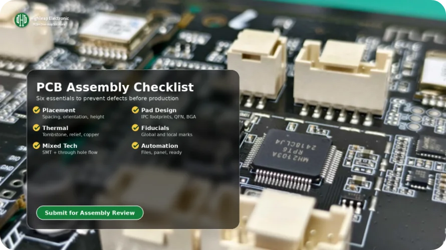
PCB Assembly Design Rules for DFM and Automated Assembly

Table of Contents
- Component Placement Rules
- Pad Design Requirements
- Thermal Design Considerations
- Fiducials and Alignment Features
- Mixed Technology Guidelines
- Design for Automated Assembly
At Highleap Electronics, we verify designs against these rules during our free DFM review. Following these guidelines helps ensure first-pass assembly success.
1) Component Placement Rules
Proper component placement enables efficient automated assembly and prevents defects.
1.1 Component Spacing Requirements
| Spacing Type | Minimum | Recommended |
|---|---|---|
| SMD to SMD (same side) | 0.5mm | 0.75mm |
| SMD to PTH | 1.0mm | 1.5mm |
| PTH to PTH | 1.5mm | 2.0mm |
| Component to board edge | 2.0mm | 3.0mm |
| Component to rail edge (panel) | 3.0mm | 5.0mm |
1.2 Component Orientation
Consistent orientation improves inspection and reduces placement errors:
- Polarized components: Same polarity direction across board
- ICs: Pin 1 in consistent corner (typically upper-left)
- Chip components: Align parallel to board edges when possible
- Connectors: Consider mating direction and cable routing
Orientation for reflow:
- Perpendicular orientation prevents component shifting (wave effect)
- Small components near board edge: long axis perpendicular to edge
1.3 Component Height Considerations
For reflow soldering:
- Keep tall components away from small ones (2mm+ clearance)
- Tall components can shadow adjacent small parts
- Consider reflow direction when placing tall components
For automated placement:
- Place tall components after low-profile
- Maximum height typically 25mm for standard equipment
- Very tall components may require manual placement
2) Pad Design Requirements
Pad design affects solder joint quality and long-term reliability.
2.1 SMD Pad Sizing
Pad dimensions should match component specifications. General guidelines:
Chip components (0402 and larger):
- Pad length: 1.0× to 1.2× terminal length
- Pad width: Equal to or slightly wider than component width
- Toe extension: 0.25-0.5mm beyond component body
- Heel extension: 0.25mm minimum
Fine-pitch ICs:
- Use manufacturer-recommended footprints
- Consider IPC-7351 pad patterns
- Verify footprint against actual component
2.2 QFN/DFN Pad Design
QFN devices require special attention:
Peripheral pads:
- Pad length: Land pattern extends 0.25-0.5mm beyond package edge
- No solder mask between pads and thermal pad
Thermal pad:
- Size: 80-90% of component thermal pad area
- Via array: 0.3mm vias on 1.0-1.2mm grid
- Via fill: Required to prevent solder wicking
- Solder mask: Opening slightly smaller than pad
2.3 BGA Pad Design
Pad type:
- NSMD (Non-Solder-Mask-Defined): Preferred for fine pitch
- SMD (Solder-Mask-Defined): Used for large pitch, better adhesion
Pad diameter:
- NSMD: 75-80% of ball diameter
- Mask opening: Pad diameter + 0.1mm minimum
Via considerations:
- Via-in-pad acceptable with fill and cap
- Dog-bone routing for larger pitch BGAs
- See stencil aperture guidelines for paste coverage
3) Thermal Design Considerations
Thermal balance prevents assembly defects during reflow.
3.1 Preventing Tombstoning
Tombstoning occurs when one end of a chip component lifts during reflow due to unequal solder surface tension.
Prevention strategies:
- Balance thermal mass at both pads
- Symmetric trace routing to pads
- Add thermal relief if one pad connects to plane
- Avoid running traces under chip components
3.2 Thermal Relief Design
For plane connections:
- Use thermal relief spokes (4 spokes typical)
- Spoke width: 0.25-0.3mm minimum
- Air gap: 0.25mm minimum
When thermal relief is needed:
- SMD pads connecting to internal planes
- PTH pads with plane connections
- Any pad requiring solder reflow/wave
3.3 Managing Large Copper Areas
Large copper areas (thermal pads, heatsinks) affect reflow:
- Preheat adequacy: Ensure reflow profile reaches all areas
- Paste coverage: Reduce paste on large thermal pads to prevent floating
- Via array: Helps conduct heat, requires filled vias
4) Fiducials and Alignment Features
Fiducials enable automated optical alignment for component placement.
4.1 Global Fiducials
Requirements:
- Minimum 3 per board/panel (2 diagonal + 1 for orientation)
- Located in panel rails for panelized boards
- Asymmetric placement prevents 180° orientation errors
Specifications:
- Pad diameter: 1.0mm typical (0.5mm-2.0mm acceptable)
- Solder mask opening: 2× pad diameter
- Clearance from other features: 3mm minimum
- Copper finish: Same as board (not covered by solder mask)
4.2 Local Fiducials
Local fiducials improve placement accuracy for fine-pitch components.
When required:
- Components with pitch ≤0.5mm
- BGAs with ball pitch ≤0.8mm
- Components requiring tighter placement tolerance
Placement:
- Two fiducials per component (diagonal corners)
- Within 50mm of component
- Not shared between components
4.3 Tooling Holes
For panel handling:
- Diameter: 3.0-4.0mm typical (non-plated)
- Location: In panel rails, symmetrically placed
- Clearance: 5mm from board edge
5) Mixed Technology Guidelines
Boards with both SMT and through-hole require special consideration.
5.1 Process Sequence
Typical mixed-technology flow:
- SMT Side 1: Paste print → Place → Reflow
- SMT Side 2 (if applicable): Paste print → Place → Reflow
- Through-hole: Insert → Wave or selective solder
- Manual assembly (if any)
5.2 Wave Solder Considerations
Component orientation:
- Long axis perpendicular to wave direction
- Connectors trailing edge (last to exit wave)
SMT on wave side:
- Limited to components rated for wave temperature
- Glue required to hold components during wave
- Avoid small pitch and BGAs on wave side
5.3 Selective Soldering
Selective soldering enables through-hole with SMT on same side:
Design for selective:
- Clearance around THT pads for nozzle access
- Group THT components when possible
- Consider solder thieves for thermal mass balance
6) Design for Automated Assembly
Optimizing for automation reduces cost and improves quality.
6.1 Component Selection
Prefer automation-friendly components:
- Standard tape-and-reel packaging
- Consistent component bodies
- Clear polarity markings
- Manufacturer-recommended footprints
Avoid or minimize:
- Odd-form components requiring manual placement
- Non-standard packaging
- Components too small (0201) or too large for equipment
6.2 Design File Requirements
Complete file package enables efficient assembly:
- Gerbers: Complete fabrication data
- Pick and place file: Component coordinates for placement
- Centroid file: XY coordinates, rotation, side
- BOM: Complete with manufacturer part numbers
- Assembly drawing: Component placement reference
See PCB assembly file requirements for complete specifications.
6.3 Panel Design
Proper panelization improves assembly efficiency:
- Consistent board orientation
- Rail dimensions matching equipment
- Fiducials and tooling in rails
- Adequate clearance from routing/V-score
See panelization requirements for SMT for detailed guidelines.
6.4 Getting Design Review
Submit your design to Highleap Electronics for free DFM review. Our engineers verify your design against these rules and provide a detailed DFM report. Use our PCB DFM checklist to self-verify before submission, and review DFT guidelines for testability requirements. Contact our engineering team to discuss any design questions or special requirements.

Charles has over 10 years of experience in PCB CAM engineering and electronics manufacturing, specializing in PCB file verification, DFM analysis, and production preparation for multilayer, HDI, RF, and high-speed boards. Proficient in Genesis, InCAM, and CAM350, he ensures accurate data, stable processes, and high manufacturing yield.
At Highleap Electronics, he focuses on process optimization and manufacturability evaluation to help customers reduce risks, shorten lead times, and achieve reliable production results.

Recommended Posts
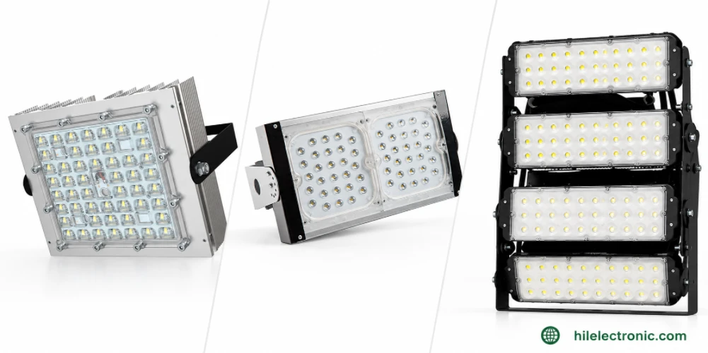
LED Parking Lot Light PCB Manufacturing & Assembly by Highleap Electronics
Figure 1. LED parking lot light PCB production and...
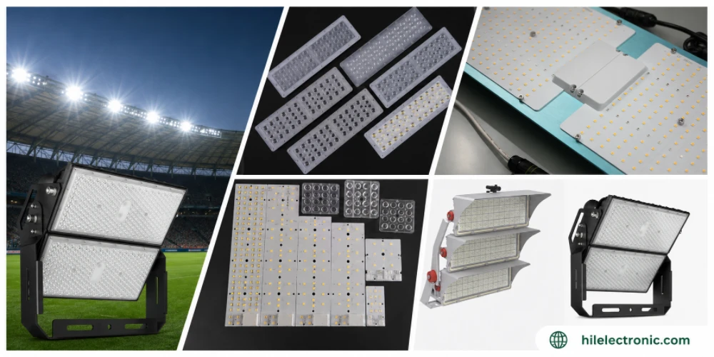
LED Stadium Light PCB Manufacturing — Very-High-Power Engines & Flicker-Free Drivers
Figure 1. LED stadium light PCB production and assembly...
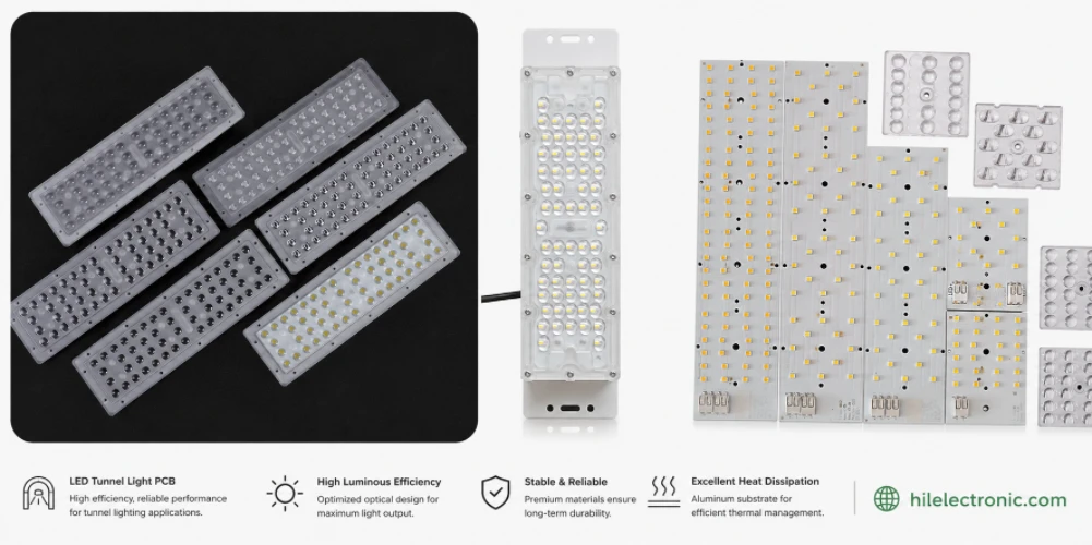
LED Tunnel Light PCB Manufacturing — High-Reliability Engines & Drivers
Figure 1. LED tunnel light PCB production and assembly...

LED Street Light PCB Manufacturing & Assembly by Highleap Electronics
Figure 1. LED street light PCB production and assembly...
How to get a quote for PCBs
Let us run DFM/DFA analysis for you and get back to you with a report.
You can upload your files securely through our website.
We require the following information in order to give you a quote:
-
- Gerber, ODB++, or .pcb, spec.
- BOM list if you require assembly
- Quantity
- Turn time
In addition to PCB manufacturing, we offer a comprehensive range of electronic services, including PCB design, PCBA (Printed Circuit Board Assembly), and turnkey solutions. Whether you need help with prototyping, design verification, component sourcing, or mass production, we provide end-to-end support to ensure your project’s success. For PCBA services, please provide your BOM (Bill of Materials) and any specific assembly instructions. We also offer DFM/DFA analysis to optimize your designs for manufacturability and assembly, ensuring a smooth production process.